EasyManua.ls Logo

Renesas M16C Series User Manual

Renesas M16C Series
380 pages
To Next Page IconTo Next Page
To Previous Page IconTo Previous Page
Page #42 background imageLoading...
Page #42 background image
Clock-Generating Circuit
M30240 Group
Rev.1.00 Sep 24, 2003 Page 24 of 360
• fAD
This clock has the same frequency as the main clock and is used for A-D conversion.
• fUSB
This is the 48mHz clock that is used for USB operation. This clock is generated from the main clock
by the frequency synthesizer circuit.
1.2.6.3 Clock Output
In single-chip mode, the clock output function select bits (bits 0 and 1 at address 0006
16
) enable f8 or
f32 to be output from the P37/CLK
OUT
pin. When the WAIT peripheral function clock stop bit (bit 2 at
address 0006
16
) is set to “1”, the output of f8 and f32 stops when a WAIT instruction is executed.
Figure 1.13 shows the system clock control registers 0 and 1.
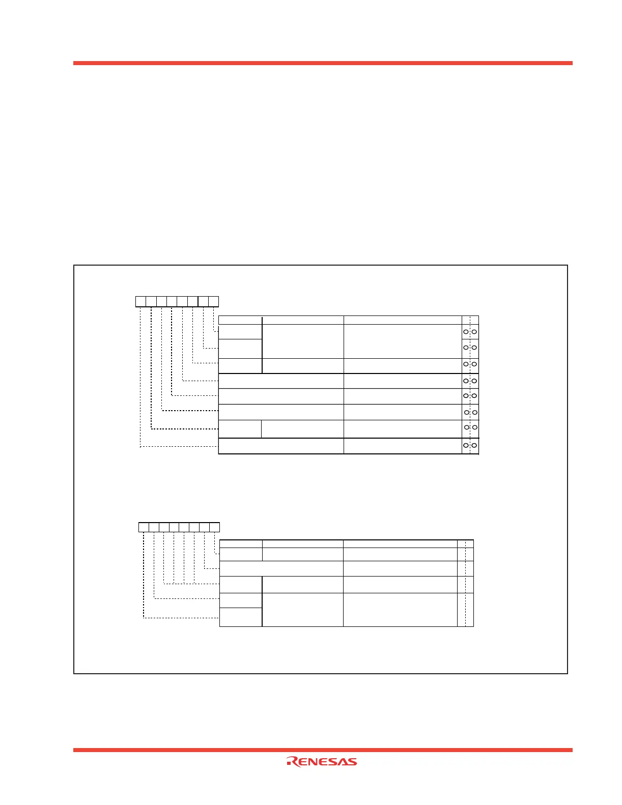
Figure 1.13: System clock control registers 0 and 1
System clock control register 0 (Note 1)
System clock control register 1 (Note 1)
Symbol Address When reset
CM1 0007
16
20
16
Bit name FunctionBit symbol
b7 b6 b5 b4 b3 b2 b1 b0
CM10 All clock stop control bit
0 : Clock on
1 : All clocks off (stop mode)
CM15
X
IN
-X
OUT
drive capacity
select bit (Note 2)
0 : LOW
1 : HIGH
WR
CM16
CM17
Main clock division select
bit 1 (Note 3)
0 0 : No division mode
0 1 : Division by 2 mode
1 0 : Division by 4 mode
1 1 : Division by 16 mode
b7 b6
00
Reserved bit
Always set to
“0”
00
Symbol Address When reset
CM0 0006
16
48
16
Bit name FunctionBit symbol
b7 b6 b5 b4 b3 b2 b1 b0
0 0 : I/O port P37
0 1 : Invalid
1 0 : f
8 output
1 1 : f
32 output
b1 b0
CM01
CM02
CM00
Clock output function
select bit
WAIT peripheral function
clock stop bit
0 : Do not stop f1, f8, f32 in wait mode
1 : Stop f
1, f8, f32 in wait mode
WR
CM06
Main clock division select
bit 0 (Note 2)
0 : CM16 and CM17 valid
1 : Division by 8 mode
Reserved bit
Always set to "1"
Reserved bit
Always set to "0"
Reserved bit
Always set to "0"
Reserved bit
Always set to "0"
o
o
o
o
o
o
o
o
Note 1: Set bit 0 of the Protect register (address 000A
16
) to "1" before writing to this register.
Note 2: Changes to "1" when shifting to stop mode.
Note 3: Can be selected when bit 6 of the System clock control register 0 (address 0006
16
) is "0".
If "1", division mode is fiixed at "8".
Note 1: Set bit 0 of the Protect register (address 000A
16
) to "1" before writing to this register.
Note 2: Changes to "1" when shifting to stop mode.

Table of Contents

Question and Answer IconNeed help?

Do you have a question about the Renesas M16C Series and is the answer not in the manual?

Renesas M16C Series Specifications

General IconGeneral
Architecture16-bit
CoreM16C
Instruction Set ArchitectureCISC
Flash MemoryUp to 512 KB
Operating Voltage2.7V to 5.5V
Operating Temperature Range-40°C to +85°C
Package TypesLQFP, QFP
TimersMultiple 16-bit timers
ADC10-bit
Communication InterfacesUART, SPI, I2C
InterruptsMultiple interrupt sources

Summary

Chapter 1: Hardware

1.1 Description

Overview of the M30240 group as a single-chip USB peripheral microcontroller based on M16C family.

1.1.1 Features

Lists the key features of the M30240 group, including CPU, USB capabilities, memory, voltage, and peripherals.

1.1.3 Pin Configuration

Shows the pin configuration (top view) of the M30240 group, detailing each pin's name, I/O, and basic function.

1.1.4 Block Diagram

Presents a block diagram illustrating the internal structure and major components of the M30240 group.

1.1.5 Performance outline

Details the performance specifications of the M30240 group, including instruction count, memory capacity, and I/O ports.

1.1.6 Pin Description

Provides a detailed description of each pin of the M30240 microcontroller, including its name, I/O type, and functions.

CHAPTER 2: PERIPHERAL FUNCTIONS USAGE

2.1 Protect

Explains the protect function to prevent unintended changes to important registers when a program runs away.

2.2 Timer A

Provides an overview and detailed operation modes of the 16-bit Timer A, including timer, event counter, and PWM modes.

2.3 Timer B

Details the operation and registers of Timer B, a 16-bit timer that operates only in timer mode.

2.4 Clock-Synchronous Serial I/O

Explains clock-synchronous serial communication, including transmission/reception formats, transfer rates, and error detection.

2.5 Clock-Asynchronous Serial I/O (UART)

Covers UART operations, including transmission/reception formats, transfer rates, error detection, and functions like SIM interface compliance.

2.6 A-D Converter

Describes the A-D converter, its modes of operation, conversion clock, conversion time, and related registers.

2.7 DMAC

Explains the DMAC (Direct Memory Access Controller) for data transfer between memory and peripherals without CPU intervention.

2.10 Address Match Interrupt

Explains the address match interrupt functionality for simplified debugging, including enable/disable and timing.

2.11 Key-Input Interrupt

Describes the key-input interrupt, which is generated by falling edges on Port 0 or Port 1 pins used as input.

2.12 Power Control

Explains power control modes (Normal, Wait, Stop) for reducing CPU power consumption by stopping oscillators or clocks.

2.13 Programmable I/O Ports

Details the programmable I/O ports, including direction registers, port registers, pull-up control, and high drive capacity.

Chapter 3 Universal Serial Bus

3.1 Frequency Synthesizer

Explains how to set up and use the frequency synthesizer to generate the 48MHz clock for USB and DC-DC converter power.

3.2 Universal Serial Bus

Provides an overview of the Universal Serial Bus (USB) features, including specification compatibility, error handling, and transfer types.

3.2.2 USB Related Registers

Lists and describes USB-related registers for controlling USB functionality, including control, status, and enable registers.

3.2.7 USB Interrupts

Details the types of USB interrupts (Function, Reset, Resume, SOF, Suspend) and their handling via enable flags and priority levels.

3.2.8 USB Function Control Unit Initialization

Outlines the initialization routine for the USB Function Control Unit, including frequency synthesizer setup and endpoint initialization.

3.2.9 USB Control Transfers and SET_ADDRESS Request

Explains USB control transfers, the SET_ADDRESS request, and procedures for setting the device address.

Chapter 4 Interrupts

4.1 Overview of Interrupts

Provides an overview of interrupt types, including software, hardware, special, and peripheral I/O interrupts.

4.1.1 Type of Interrupts

Classifies interrupts into maskable and non-maskable types, detailing software and hardware interrupt categories.

4.1.2 Interrupt Vector Tables

Describes interrupt vector tables, including fixed and variable types, and lists interrupts assigned to fixed vector tables.

4.1.3 Interrupt Control

Explains interrupt control registers, interrupt request bits, enable flags, and priority levels for managing interrupts.

4.1.4 Interrupt Sequence

Details the sequence of operations when an interrupt occurs, including saving registers and processor control flow.

4.1.5 Multiple Interrupts

Explains how multiple interrupts are handled, including priority levels and interrupt acceptance conditions.

Chapter 5 Built-in PROM Version

5.1 Built-in PROM Version

Introduces the built-in PROM version, its functions, and available types (OTP and EPROM).

5.1.1 Outline

Outlines the capabilities of the built-in PROM version, including programming methods and suitability for different production volumes.

5.2 EPROM version

Describes the EPROM version, its operating modes (Normal, EPROM), and related pins.

5.2.1 EPROM mode pins

Lists pin functions specifically for the EPROM mode, detailing their roles in programming and verification.

5.2.2 Input/Output signals

Explains the input/output signals for Read, Program, and Erase operations in EPROM mode.

5.2.3 Algorithm Programming

Details the step-by-step algorithm for programming the built-in PROM, including voltage settings and pulse application.

5.3 Usage Precaution

Provides precautions for using built-in PROM versions, including handling of high voltage and protection of the EPROM window.

5.3.1 Built-in PROM versions

Offers specific cautions for programming built-in PROM versions, emphasizing voltage and power-on sequences.

5.3.2 One-time PROM versions

Highlights that OTP versions are not tested/screened, recommending programming and testing for reliability.

5.3.3 EPROM versions

Advises on protecting the EPROM window from light and cleaning it before erasure for optimal performance.

Chapter 6 Standard Characteristics

6.1 Standard DC Characteristics

Presents standard DC characteristics of the M30240EC, including output currents and voltage ratings.

Related product manuals