RL78/F13, F14 CHAPTER 34 ELECTRICAL SPECIFICATIONS (GRADE L)
R01UH0368EJ0210 Rev.2.10 1718
Dec 10, 2015
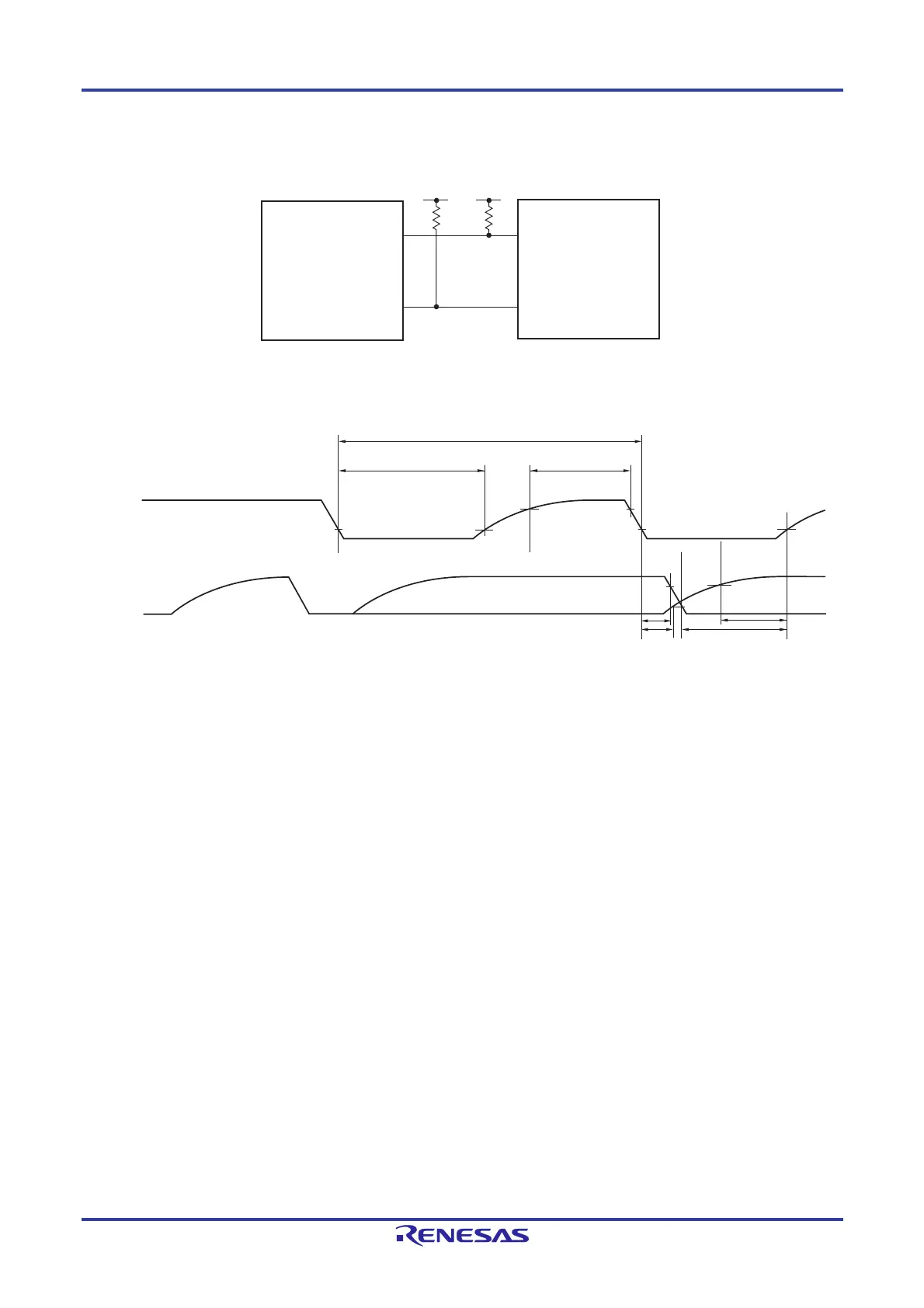
Simplified I
2
C mode connection diagram (during communication at different potential)
Simplified I
2
C mode serial transfer timing (during communication at different potential)
Caution Select the TTL input buffer and the N-ch open-drain output mode for the SDAr pin and N-ch open-drain
output mode for the SCLr pin.
Remarks 1. R
b [Ω]: Communication line (SDAr, SCLr) pull-up resistance, Cb [F]: Communication line (SDAr, SCLr) load
capacitance, V
b [V]: Communication line voltage
2. f
MCK: Serial array unit operation clock frequency
SDAr
SCLr
SDA
SCL
User's device
Vb
Rb
Vb
Rb
RL78
microcontroller
SDAr
t
LOW
t
HIGH
t
HD : DAT
SCLr
t
SU : DAT
1/f
SCL
 Loading...


