RL78/F13, F14 CHAPTER 6 TIMER ARRAY UNIT
R01UH0368EJ0210 Rev.2.10 430
Dec 10, 2015
6.2 Configuration of Timer Array Unit
Timer array unit includes the following hardware.
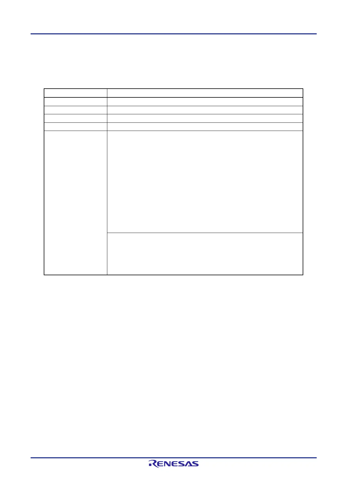
Table 6-1. Configuration of Timer Array Unit
Item Configuration
Timer/counter Timer count register mn (TCRmn)
Register Timer data register mn (TDRmn)
Timer input
TI00 to TI07, TI10 to TI17
Note 1
, RxD0 pin (for LIN-bus)
Timer output
TO00 to TO07, TO10 to TO17 pins
Note 1
, output controller
Control registers <Registers of unit setting block>
Peripheral enable register 0 (PER0)
Timer clock select register m (TPSm)
Timer channel enable status register m (TEm)
Timer channel start register m (TSm)
Timer channel stop register m (TTm)
Timer input select register 0 (TIS0)
Timer input select register 1 (TIS1)
Timer input select register 2 (TIS2)
Timer output enable register m (TOEm)
Timer output register m (TOm)
Timer output level register m (TOLm)
Timer output mode register m (TOMm)
PWM output delay control register 1 (PWMDLY1)
PWM output delay control register 2 (PWMDLY2)
Note 3
<Registers of each channel>
Timer mode register mn (TMRmn)
Timer status register mn (TSRmn)
Noise filter enable registers 1, 2 (NFEN1, NFEN2)
Port mode register (PMxx)
Note 2
Port register (Pxx)
Note 2
Notes 1. The presence or absence of timer I/O pins of channel 0 to 7 of the unit depends on the product. See Table 6-
2 Timer I/O Pins provided in Each Product for details.
2. The port mode registers (PMxx) and port registers (Pxx) to be set differ depending on the product. For details,
see 6.3.16 Port mode registers 1, 3, 4, 7, 12 (PM1, PM3, PM4, PM7, PM12).
3. Bit allocation differs depending on the group.
Remark m: Unit number (m = 0, 1), n: Channel number (n = 0 to 7)
 Loading...


