RL78/F13, F14 CHAPTER 4 PORT FUNCTIONS
R01UH0368EJ0210 Rev.2.10 285
Dec 10, 2015
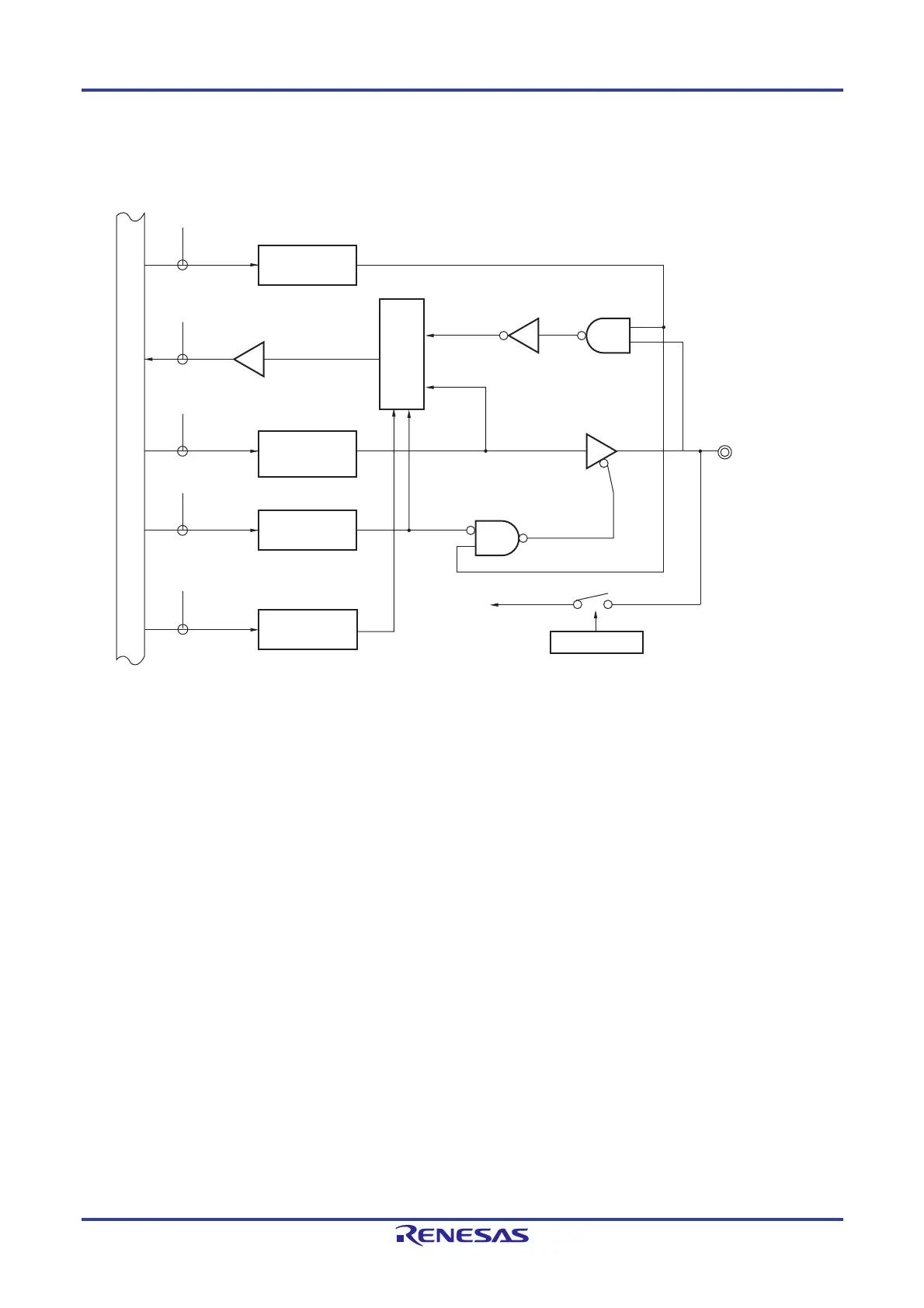
Figures 4-58 to 4-60 show block diagrams of port 10 for 100-pin products.
Figure 4-58. Block Diagram of P100 to P105
P100/ANI18,
P101/ANI19,
P102/ANI20,
P103/ANI21,
P104/ANI22,
P105/ANI23
WR
ADPC
RD
WR
PORT
WR
PM
ADPC
PM10
P10
PM100 to PM105
P100 to P105
ADPC4 to ADPC0
WR
PMS
PMS
PMS0
0: Analog input
1: Digital I/O
Internal bus
Output latch
Selector
A/D converter
ADS
ADS4 to ADS0
P10: Port register 10
PM10: Port mode register 10
PMS: Port mode select register
ADPC: A/D port configuration register
ADS: Analog input channel specification register
RD: Read signal
WRxx: Write signal
 Loading...


