Configurable logic
ABB Network Partner AB
1MRK 580 161-XEN
Page 4 - 27
Version 1.0-00
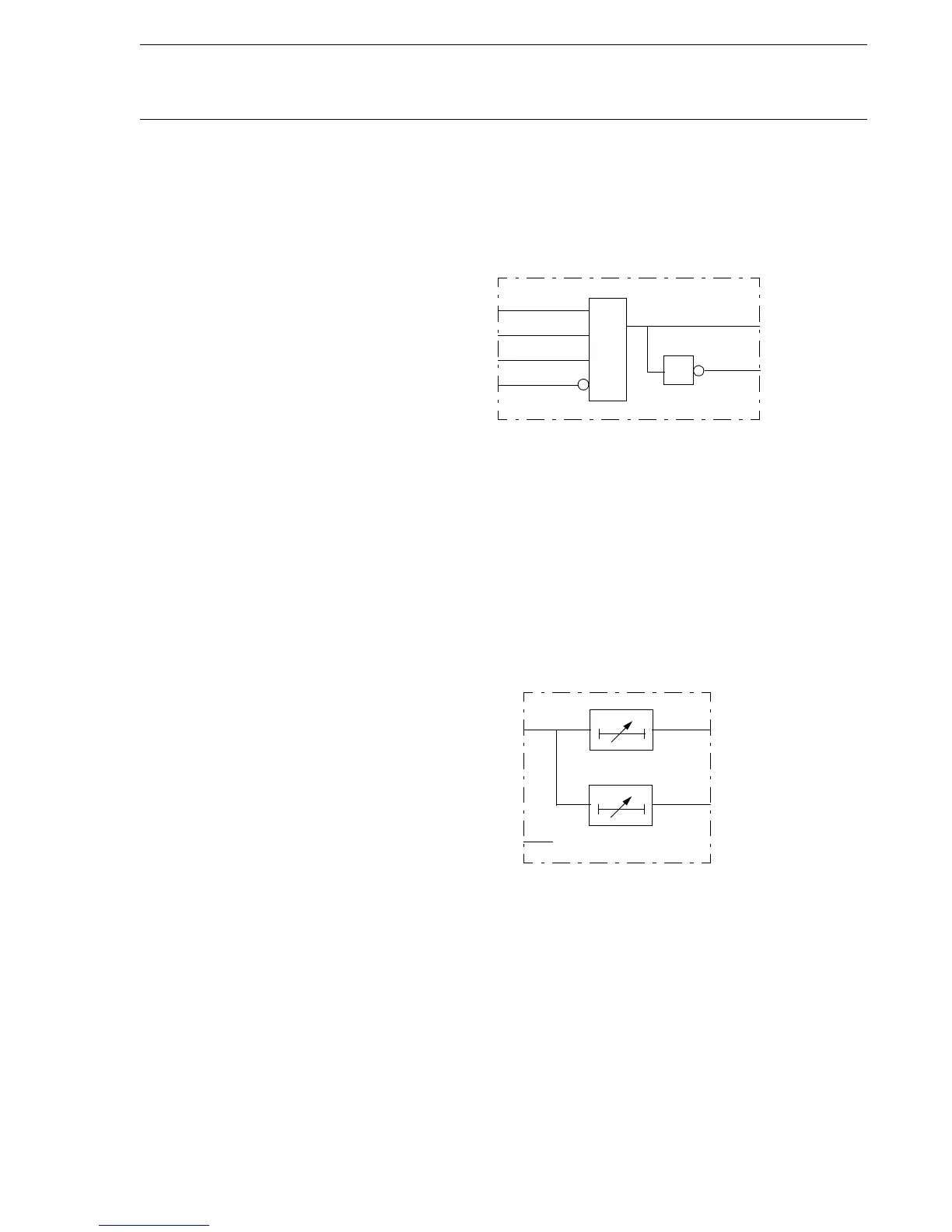
2.3 AND The configuration logic AND gate (Fig. 3) has four inputs (one of them
inverted), designated Annn-INPUTm (Annn-INPUT4N is inverted), where
nnn runs from 001 to 010 for REL 531 and to 249 for REC 561 and
presents the serial number of the block, and m presents the serial number
of the inputs in the block. Each AND circuit has two outputs, Annn-OUT
and Annn-NOUT (inverted).
Fig. 3 Block diagram of the AND function
2.4 Timer The configuration logic TM timer, delayed at pick-up and at drop-out (Fig. 4)
has a settable time delay TMnn-T between 0 and 50.00 s in steps of 0.01 s.
The input signal for each time delay block has the designation TMnn-
INPUT, where nn runs from 01 to 10 and presents the serial number of the
logic block. The output signals of each time delay block are TMnn-ON
and TMnn-OFF. The first one belongs to the timer delayed on pick-up and
the second one to the timer delayed on drop-out. Both timers within one
block always have the same setting.
Fig. 4 Block diagram of the Timer function
INPUT1
INPUT2
INPUT3
INPUT4N
Annn
1
OUT
NOUT
&
(X80161-3)
t
t
Time delay 0-50.00 s
INPUT
T
OFF
ON
TMnn
(X80161-4)
 Loading...