When a latch output is enabled, segments in the selected digit
are turned on.
Digit selection is performed by data from the PA3, I’A4, and
PA5 outputs of the MPU to control U203. A single U203 out-
put, corresponding to the selected digit, will go low when the
correct data appears on its inputs. For example, if 0102 ap-
pears on the inputs of U203, DS201 will be turned on.
Selection of the display annunciators is performed in a similar
manner. The data stored in the corresponding segment lat-
ches will then turn on the appropriate annunciator LEDs.
Front panel switches are read in a somewhat similar manner
by using a row-column matrix along with U206. To select a
particular row, data is transmitted out the MPU PA3, PA4,
and PA5 lines to U206. This action selects one of the rows by
placing the corresponding output of U206 high. Matrix col-
umns are then read by reading data in through PAO, PAl.
and PAZ, of the MPU. If a particular switch contact is closed,
the data bit will be high; if the switch is open, the data bit will
be low.
6.7 VOLTAGE SOURCE
The voltage source circuitry, which is located on schematic
number 617-106, page 1, consists of serial-to-parallel data
conversion circuitry,
the DAC (Digital-to-Analog
Converter), analog circuitry, current limit circuitry, and pro-
tection circuitry.
Incoming clock and data signals are fed in through opto-
isolators U123 and U124 respectively. The 88.92kHz clock is
further divided down by U132. The pulse width modulated
serial data controls the reset pin of U132. The Q2 and Q3 out-
puts of the divider are used to control the data and strobe in-
puts of the serial-to-parallel converter ICs, U131 and U140.
Control information consists of 12 bit words. As the bits
come in, they are fed into the DATA input of U131 and U140
in serial form. After all bits are shifted in, data is strobed into
the outputs of U131 and U140.
The resulting 12 bit data is then applied to the digital inputs of
U141, a 12 bit DAC (Digital-to-Analog Converter). This IC
converts the digital information into an analog current out-
put. The current output of U141 is then converted into a
flOV full scale signal by U142A and U142B. The circuit is
configured so that +lOV will appear at the output of U142B
when all cmes appear on the digital inputs of the DAC. Con-
versely, - 1OV will appear at the output of U142B when all
zeroes appear on the digital inputs of the DAC.
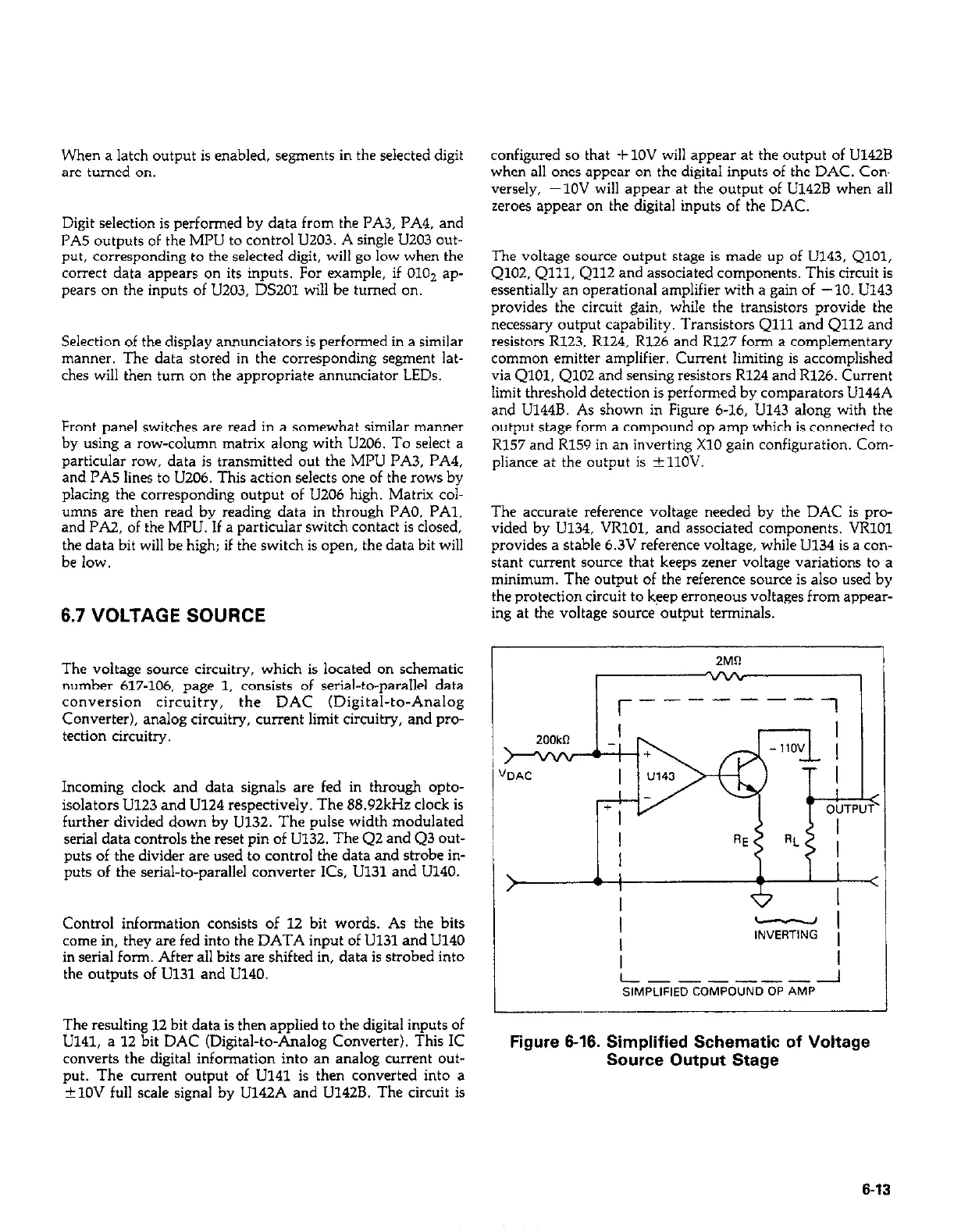
The voltage source output stage is made up of U143, QlOl,
Q102. Qlll, Qll2 and associated components. This circuit is
essentially an operational amplifier with a gain of -10. U143
provides the circuit gain, while the transistors provide the
necessary output capability. Transistors Qlll and Qll2 and
resistors R123, R124, R126 and R127 form a complementary
ccmmmn emitter amplifier. Current limiting is accomplished
via QlOl, QlO2 and sensing resistors R124 and R126. Current
limit threshold detection is performed by comparators LJ144A
and U144B. As shown in Figure 6-16, U143 along with the
output stage form a compound op amp which is connected to
R157 and R159 in an inverting X10 gain configuration. Com-
pliance at the output is ?llOV.
The accurate reference voltage needed by the DAC is pro-
vided by U134, VRlOl, and associated components. VI7101
provides a stable 6.3V reference voltage, while U134 is a con-
stant current wurce that keeps zener voltage variations to a
minimum. The output of the reference source is also used by
the protection circuit to keep ernmecu voltages from appear-
ing at the voltage source output terminals.
I
-I
I
INVERTING ,
I
I
L---------I
SIMPLIFIED COMPOUND DP AMP
J
Figure 6-16. Simplified Schematic of Voltage
Source Output Stage
6-13
 Loading...