REFERENCE
PHASE
SIGNAL
PHASE
CALCULATE
A READING
COMMON
PHASE
SIGNAL
PHASE
CALCULATE
A READING
Figure 6-13 Multiplexer Phases
6.4.3 -2V Reference Source
Model 617 measurements are based on comparing the
unknown signal with an internal -2V reference voltage
source. During each measurement cycle, the unknown signal
is sampled and then compared with signal common and the
-2v reference values.
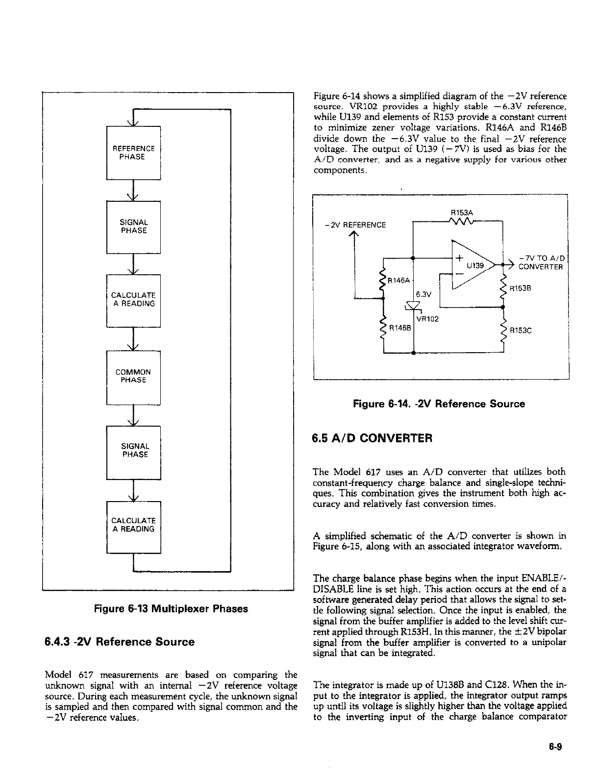
Figure 6-14 shows a simplified diagram of the -2V reference
source. VR102 provides a highly stable -6.3V reference,
while U139 and elements of R153 provide a constant current
to minimize zener voltage variations. R146A and R146B
divide down the -6.3V value to the final -2V reference
voltage. The output of U139 (- 7V) is used as bias for the
A/D converter, and as a negative supply for various other
-2”
i
R153A
REFERENCE I
-7” TO A,[
CR102
Figure 6-14. -2V Reference Source
6.5 A/D CONVERTER
The Model 617 uses an A/D converter that utilizes both
constant-frequency charge balance and single-slope techni-
ques. This combination gives the instrument both high ac-
curacy and relatively fast conversion times.
A simplified schematic of the A/D converter is show” in
Figure 6-15, along with an associated integrator waveform.
The charge balance phase begins when the input ENABLE/-
DISABLE line is set high. This action occurs at the end of a
software generated delay period that allows the signal to set-
tle following signal selection. Once the input is enabled, the
signal from the buffer amplifier is added to the level shift cur-
rent applied through R153H. In this manner, the k2V bipolar
signal from the buffer amplifier is converted to a unipolar
signal that can be integrated.
The integrator is made up of U138B and C128. When the in-
put to the integrator is applied, the integrator output ramps
up until its voltage is slightly higher than the voltage applied
to the inverting input of the charge balance comparator
6-9
 Loading...