September 5, 2008 6881076C25-E
4-18 Troubleshooting Procedures: VCO Procedures
4.3.3 800 MHz Band
Use these instructions along with the Theory of Operation, the block diagram, and the schematic to
help isolate failures, first, to the individual circuits, and finally to the failing piece part.
4.3.3.1 VCO Hybrid Assembly
The VCO hybrid substrate is glued to the carrier board. The hybrid is not a field-repairable assembly.
If a failure is indicated in this assembly, replace the entire carrier board.
4.3.3.2 Out-of-Lock Condition
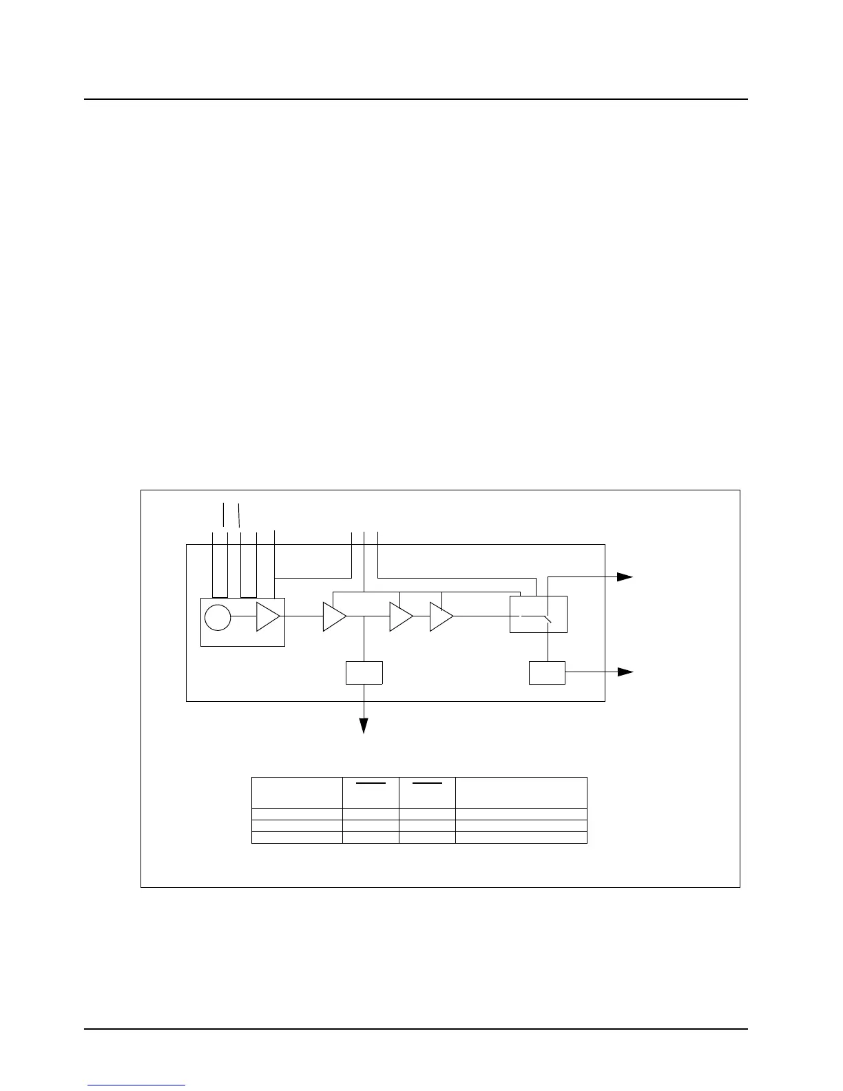
The probable cause of an out-of-lock condition is a failure in the synthesizer circuit. (See
Section 4.1.4.2 on page 4-7.) If the voltages on the AUX 1* and AUX 2* lines do not conform to the
table in Figure 4-3, troubleshoot the synthesizer.
If the AUX 1* and AUX 2* voltages are correct but the synthesizer feedback level is not within the
range indicated, troubleshoot the first buffer on the VCO carrier board. If no problem is found with the
first buffer and the level out of the VCO is below that indicated on the block diagram, check J straps
MP9656-MP9668. If no problem is found with these, replace the entire carrier board.
If the AUX 1* and AUX 2* voltages are correct and the synthesizer feedback level is correct but an
out-of-lock condition persists, troubleshoot the synthesizer.
Figure 4-3. VCO Block Diagram – 800 MHz Band
FREQUENCY
RANGE
AUX1
AUX2 OUTPUT FREQUENCY
RX HI HI 741.35 – 759.35
TX HI LOW 806.00 – 824.00
TA LOW LOW 851.00 – 869.00
OSC
VCO HYBRID
+1.0 dBm
Min
1ST
BUFFER
PAD
DOUBLER
2ND
BUFFER
PAD
CARRIER BOARD SYNTH FEEDBACK RX INJ
RX = 370.675 - 379.675
TX = 403.000 - 412.000
TA = 425.500 - 434.500
6.0 dBm + 7 dBm
-
-
GPW-6395-O
TX/RX
SWITCH
TX
INJ
741.35 - 759.35
TX = 806 - 824
TA = 851 - 869
+
S
L
A
U
X
1
A
U
X
2
8
.
6
-
S
L
9
.
6
K
9
.
4
MOD
 Loading...