6881076C25-E September 5, 2008
Theory of Operation: ASTRO Spectra VOCON Board 3-21
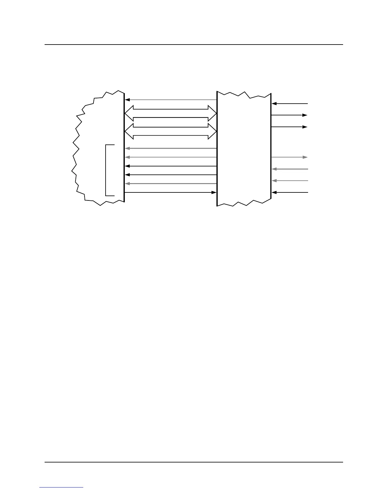
3.3.5 TX Signal Path
The transmit signal path follows some of the same design structure as the receive signal path
described in Section 3.3.4, "RX Signal Path," on page 3-18 (refer to Figure 3-10). It is advisable to
read through the section on RX Signal Path that precedes this section.
Figure 3-10. DSP RSSI Port – TX Mode
The ADSIC contains a microphone A/D with a programmable attenuator for coarse level adjustment.
As with the speaker D/A attenuator, the microphone attenuator value is programmed by the MCU
through the SPI bus. The analog microphone signal from the command board is input to the A/D on
MAI (Mic Audio In). The microphone A/D converts the analog signal to a digital data stream and
stores it in internal registers. The DSP accesses this data through the parallel configuration bus
consisting of D8–D23, A0–A2, A13–A15, RD*, and WR*. As with the speaker data samples, the DSP
reads the microphone samples from registers mapped into it's memory space starting at Y:FFF0.
The ADSIC provides an 8 kHz interrupt to the DSP on IRQB for processing these microphone data
samples.
As with the received trunking low-speed data, low speed Tx data is processed by the MCU and
returned to the DSP at the DSP SCLK port connected to the MCU port PA0.
For secure messages, the digital signal may be passed to the secure module for encryption prior to
further processing. The DSP transfers the data to and from the secure module through its SCI port,
consisting of TXD and RXD. Configuration and mode control of the secure module is performed by
the MCU via the SPI bus.
The DSP processes these converted microphone samples, generates and mixes the appropriate
signalling, and filters the resultant data. This data is then transferred to the ADSIC IC on the DSP
SSI port. The transmit side of the SSI port consists of SC2, SCK, and STD. The DSP SSI port is a
synchronous serial port. SCK is the 1.2 MHz clock input derived from the ADSIC, which makes it
synchronous. The data is clocked over to the ADSIC on STD at a 1.2 MHz rate. The ADSIC
generates a 48 kHz interrupt on SC2 so that a new sample data packet is transferred at a 48 kHz
rate which sets the transmit data sampling rate at 48Ksp.
48KHz TX Data Interrupt
Serial Transmit Data
Serial Receive Data
2.4 MHz Receive Data Clock
20 KHz RX Data Interrupt
1.2 MHz Tx Data Serial Clock
D8-D23
A0-A2,A13-A15,RD*,WR*
SCKR
RFS
TFS
SCKT
RXD
TXD
ADSIC
U406
MAI
VVO
MODIN
J501-49
J501-39
SC0
SC1
SC2
SCK
SRD
STD
SSI
SERIAL
DSP56001
U405
IRQB
IRQB
8KHz
SBI
DIN
DIN-
IDC
ODC
Data In
Data In*
SBI
ABACUS II
Interface
J501-1
J501-2
J501-7
J501-6
VRO
REF MOD
J501-48
 Loading...