Low Band Frequency Synthesis Section 7: 2-7
6881091C63-F
4.0 Low Band Frequency Synthesis
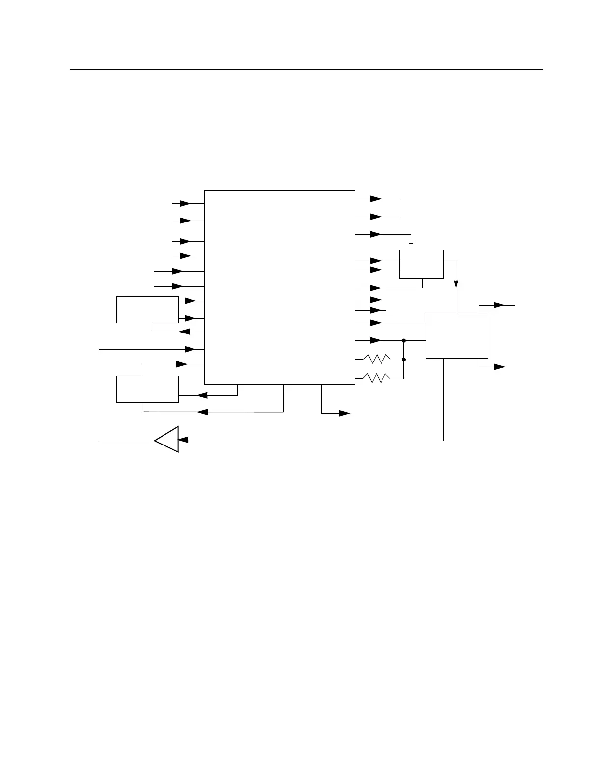
The frequency synthesizer subsystem, shown in Figure 7-3, consists of the reference oscillator
crystal (Y1201), the Low Voltage Fractional-N synthesizer (LVFRAC-N, U1201), and the receive and
transmit VCOs and buffers (Q1303 through Q1308 and associated components).
Figure 7-3 Low Band Synthesizer Block Diagram
4.1 Fractional-N Synthesizer
The LVFRAC-N synthesizer IC (U1201) consists of a reference oscillator, pre-scaler, a
programmable loop divider, control divider logic, phase detector, a charge pump, A/D converter for
low frequency digital modulation, a balance attenuator to balance high frequency analog modulation
and low frequency digital modulation, a 13V positive voltage multiplier, a serial interface for control,
and finally a super filter for the regulated 9.3 volt supply.
Regulated 9.3 volts DC applied to the super filter input (U1201, pin 30) delivers a very low noise
output voltage of 8.3 volts DC (VSF) at pin 28. External device Q1201 allows greater current
sourcing capability. The VSF source supplies the receive and transmit VCOs and first buffer stages.
The synthesizer IC supply voltage is provided by a dedicated 5V regulator (U1250) to minimize
power supply noise.
DATA
CLK
CEX
MODIN
SFIN
XTAL1
XTAL2
WARP
PREIN
VCP
REFERENCE
OSCILLATOR
VOLTAGE
MULTIPLIER
DATA (U0101 PIN 100)
CLOCK (U0101 PIN 1)
CSX (U0101 PIN 2)
MOD IN (U0221 PIN 40)
9,3V (U641 PIN 5)
7
8
9
10
30
23
24
25
32
47
VMULT2 VMULT1
BIAS1
SFOUT
AUX3
AUX4
IADAPT
IOUT
GND
FREFOUT
LOCK
4
19
6, 22, 33, 44
43
45
3
2
28
14
15
40
FILTERED 8,3V
STEERING
LOCK (U0101 PIN 56)
PRESCALER IN
FREF (U0221 PIN 34)
39
BIAS2
41
48
5, 13, 20, 34, 36
+5V (U3211 PIN 1)
AUX1
VDD, DC5V
MODOUT
U1201
LOW VOLTAGE
FRACTIONAL-N
SYNTHESIZER
AUX2
TX RF INJECTION
(1ST STAGE OF PA)
LO RF INJECTION
VOLTAGE
CONTROLLED
OSCILLATOR
LINE
2-POLE
LOOP
FILTER
1
Q1202
BUFFER
BWSELECT
VCTRL
N.C.
N.C.

 Loading...