VHF (136–174 MHz) 25–45W LDMOS Transmitter Power Amplifier (PA) 45 W Section 11: 2-3
6881091C63-F
The IF IC contains a quadrature detector using a ceramic phase-shift element (Y3102) to provide
audio detection. Internal amplification provides an audio output level of 120 mV rms (at 60%
deviation) from U3101 pin 8 (DISCAUDIO) which is fed to the ASFIC_CMP (U0221) pin 2 (part of
the Controller circuits).
A Receive Signal Strength Indicator (RSSI) signal is available at U3101, pin 5, having a dynamic
range of 70 dB. The RSSI signal is interpreted by the µP (U0101, pin 63) and in addition is available
at accessory connector J0501-15.
3.0 VHF (136–174 MHz) 25–45W LDMOS Transmitter Power
Amplifier (PA) 45 W
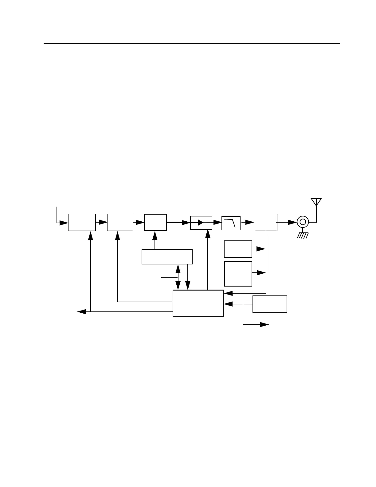
The radio’s 45W PA is a three-stage amplifier used to amplify the output from the VCOBIC to the
radio transmit level. All three stages utilize LDMOS technology. The gain of the first stage (U3401) is
adjustable, controlled by pin 4 of PCIC (U3501) via U3402-1. It is followed by an LDMOS driver
stage (Q3421) and an LDMOS final stage (Q3441). All devices are surface mounted. A pressure
pad between the board and the radio’s cover provides both closure of the switch and insurance of
good thermal contact between the devices and the chassis.
Figure 11-2 VHF LDMOS Transmitter Block Diagram
3.1 Power Controlled Stage
The first stage (U3401) is a 20 dB gain integrated circuit containing two LDMOS FET amplifier
stages. It amplifies the RF signal from the VCO (TXINJ). The output power of stage U3401 is
controlled by a DC voltage applied to pin 1 from the power control circuit (U3501 pin 4, with
operational amplifier U3402-1, pin 1). The control voltage simultaneously varies the bias of two FET
stages within U3401. This biasing point determines the overall gain of U3401 and therefore its
output drive level to Q3421, which in turn controls the output power of the PA.
Op-amp U3402-1 monitors the drain current of U3401 via resistor R3444 and adjusts the bias
voltage of U3401 so that the current remains constant. The PCIC (U3501) provides a DC output
voltage at pin 4 (INT) which sets the reference voltage of the current control loop. A rising power
Antenna
PCIC
Pin Diode
Antenna
Switch
RF Jack
Harmonic
Filter
Power
Sense
PA-Final
Stage
PA
Driver
From VCO
Controlled
Stage
Vcontrol
Bias 1
Bias 2
To Microprocessor
Temperature
Sense
SPI BUS
ASFIC_CMP
PA
PWR
SET
To Microprocessor
Current
Sense
Secondary
Temp
Sense

 Loading...