UHF Band 1 (403–470 MHz) 25–40 W Bipolar Transmitter Power Amplifier (PA) 40W Section 9: 2-3
6881091C63-F
2nd IF signal is amplified and filtered by an external pair of 455 kHz ceramic filters (FL3112, FL3114)
for 20/25 kHz channel spacing or FL3111 and FL3113/F3115 for 12.5 kHz channel spacing. These
pairs are selectable via BWSELECT. The filtered output from the ceramic filters is applied to the
limiter input pin of the IF IC (pin 14).
The IF IC contains a quadrature detector using a ceramic phase-shift element (Y3102) to provide
audio detection. Internal amplification provides an audio output level of 120 mV rms (at 60%
deviation) from U3103 pin 8 (DISCAUDIO) which is fed to the ASFIC_CMP (U0221) pin 2 (part of
the controller circuits).
A Receive Signal Strength Indicator (RSSI) signal is available at U3101 pin 5, having a dynamic
range of 70 dB. The RSSI signal is interpreted by the µP (U0101 pin 63) and is available at
accessory connector J0501-15.
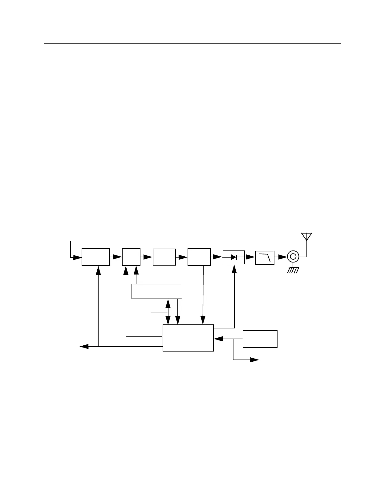
3.0 UHF Band 1 (403–470 MHz) 25–40 W Bipolar Transmitter Power
Amplifier (PA) 40W
The radio’s 40W power amplifier (PA) is a four-stage amplifier used to amplify the output from the
VCOBIC to the radio transmit level. It consists of the following four stages in the line-up. The first
stage is a LDMOS pre-driver (U4401) that is controlled by pin 4 of PCIC (U4501) via Q4473
(CNTLVLTG). It is followed by another LDMOS stage (Q4421), an LDMOS stage (Q4431), and a
bipolar final stage (Q4441).
Figure 9-2 UHF Transmitter Block Diagram
Device Q4401 is surface mounted. Q4421, Q4431 and Q4441 are directly attached to the heat sink.
3.1 Power Controlled Stage
The first stage (U4401) amplifies the RF signal from the VCO (TXINJ) and controls the output power
of the PA. The output power of the transistor U4401 is controlled by a voltage control line feed from
PCIC
Pin Diode
Antenna
Switch
RF Jack
Antenna
Harmonic
Filter
Power
Sense
PA-Final
Stage
PA
Driver
From VCO
Controlled
Stage
Vcontrol
Bias 1
Bias 2
To Microprocessor
Temperature
Sense
SPI BUS
ASFIC_CMP
PA
PWR
SET
To Microprocessor

 Loading...