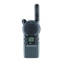
Section 13: 2-6 UHF Band 2 (450–512/520 MHz) 25–40 W LDMOS Frequency Synthesis
6881091C63-F
4.0 UHF Band 2 (450–512/520 MHz) 25–40 W LDMOS Frequency
Synthesis
The synthesizer subsystem shown in Figure 13-3, consists of the reference oscillator (Y5261 or
Y5262), the Low Voltage Fractional-N synthesizer (LVFRAC-N, U5201), and the Voltage Controlled
Oscillator (VCO).
4.1 Reference Oscillator
The reference oscillator (Y5262) contains a temperature compensated crystal oscillator with a
frequency of 16.8 MHz. An analog-to-digital (A/D) converter internal to U5201 (LVFRAC-N) and
controlled by the µP via serial interface (SRL) sets the voltage at the warp output of U5201, pin 25 to
set the frequency of the oscillator. The output of the oscillator (Y5262, pin 3) is applied to pin 23
(XTAL1) of U5201 via an RC series combination.
In applications where less frequency stability is required, the oscillator inside U5201 is used along
with external crystal Y5261, varactor diode D5261, C5261, C5262, and R5262. In this case, Y5262,
R5263, C5235 and C5251 are not used. When Y5262 is used, Y5261, D5261, C5261, C5262 and
R5262 are not used, and C5263 is increased to 0.1 uF.
4.2 Fractional-N Synthesizer
The LVFRAC-N synthesizer IC (U5201) consists of a pre-scaler, programmable loop divider, control
divider logic, phase detector, charge pump, A/D converter for low frequency digital modulation,
balanced attenuator used to balance high frequency analog modulation and low frequency digital
modulation, 13 V positive voltage multiplier, serial interface for control, and a super filter for the
regulated 5 volts.
A voltage of 5 V applied to the super filter input (U5201, pin 30) supplies an output voltage of 4.5
Vdc (VSF) at pin 28. It supplies the VCO, VCO modulation bias circuit (via R5322), and synthesizer
charge pump resistor network (R5251, R5252). The synthesizer supply voltage is provided by 5 V
regulator, U5211.
To generate a high voltage to supply the phase detector (charge pump) output stage at pin VCP
(U5701-32), a voltage of 13 Vdc is generated by the positive voltage multiplier circuit (D5201,
C5202, and C5203). This voltage multiplier is basically a diode capacitor network driven by two
signals (1.05 MHz) 180 degrees out of phase (U5201, pins 14 and 15).

 Loading...