VHF (136–174 MHz) 25–45 W Bipolar Transmitter Power Amplifier (PA) 45 W Section 8: 2-3
6881091C63-F
are selectable via BWSELECT. The filtered output from the ceramic filters is applied to the limiter
input pin of the IF IC (pin 14).
The IF IC contains a quadrature detector using a ceramic phase-shift element (Y3102) to provide
audio detection. Internal amplification provides an audio output level of 120 mV rms (at 60%
deviation) from U3101 pin 8 (DISCAUDIO) which is fed to the ASFIC_CMP (U0221) pin 2 (part of
the Controller circuits).
A Receive Signal Strength Indicator (RSSI) signal is available at U3101, pin 5, having a dynamic
range of 70 dB. The RSSI signal is interpreted by the µP (U0101, pin 63) and in addition is available
at accessory connector J0501-15.
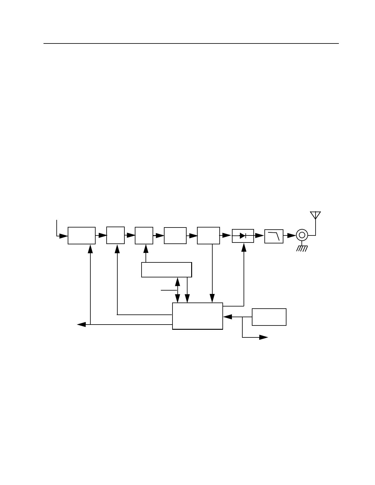
3.0 VHF (136–174 MHz) 25–45 W Bipolar Transmitter Power
Amplifier (PA) 45 W
The radio’s 45W PA is a four-stage amplifier used to amplify the output from the VCOBIC to the
radio transmit level. The line-up consists of three stages which utilize LDMOS technology, followed
by a final stage using a bipolar device. The gain of the first stage (U3401) is adjustable, controlled
by pin 4 of PCIC (U3501) via Q3501 and Q3502 (VCONT). It is followed by an LDMOS pre-driver
stage (Q3421), an LDMOS driver stage (Q3431) and a bipolar final stage (Q3441).
Figure 8-2 VHF Transmitter Block Diagram
Devices U3401 and Q3421 are surface mounted. The remaining devices are directly attached to the
heat sink.
3.1 Power Controlled Stage
The first stage (U3401) is a 20 dB gain integrated circuit containing two LDMOS FET amplifier
stages. It amplifies the RF signal from the VCO (TXINJ). The output power of stage U3401 is
controlled by a DC voltage applied to pin 1 from the power control circuit (U3501 pin 4, with
transistors Q3501 and Q3502 providing current gain and level-shifting). The control voltage
Antenna
PCIC
Pin Diode
Antenna
Switch
RF Jack
Harmonic
Filter
Power
Sense
PA-Final
Stage
PA
Driver
From VCO
Controlled
Stage
Vcontrol
Bias 1
Bias 2
To Microprocessor
Temperature
Sense
SPI BUS
ASFIC_CMP
PA
PWR
SET
To Microprocessor
Pre
Driver

 Loading...