4-5
4-2. PRINTED WIRING BOARDS AND SCHEMATIC DIAGRAMS
(Measuring conditions voltage and waveform)
• Voltages and waveforms are measured between the measure-
ment points and ground when camera shoots color bar chart of
pattern box. They are reference values and reference wave-
forms. *
(VOM of DC 10 MΩ input impedance is used.).
• Voltage values change depending upon input impedance of VOM
used.) *
1. Connection
2. Adjust the distance so that the output waveform of Fig. a and
the Fig. b can be obtain.
Yellow
AABBA=B
Fig. a (Video output terminal output waveform)
Fig.b (Picture on monitor TV)
Electron beam
scanned frame
CRT picture frame
H
Cyan
Green
White
Magenta
Red
Blue
Yellow
Cyan
Green
White
Magenta
Red
Blue
THIS NOTE IS COMMON FOR WIRING BOARDS AND SCHEMATIC DIAGRAMS
(In addition to this, the necessary note is printed in each block)
C
BE
5
64
2
13
5
46
2
31
45
2
31
12
4
53
3
21
3
21
3
21
Transistor Diode
Kinds of capacitor
Temperature characteristics
External dimensions (mm)
Note :
The components identified by
mark 0 or dotted line with mark
0 are critical for safety.
Replace only with part number
specified.
Note :
Les composants identifiés par
une marque 0 sont critiques
pour la sécurité.
Ne les remplacer que par une
pièce portant le numéro spécifié.
When indicating parts by reference number, please include
the board name.
(For printed wiring boards)
• b: Pattern from the side which enables seeing.
(The other layers' patterns are not indicated.)
• Through hole is omitted.
• Circled numbers refer to waveforms.
• There are few cases that the part printed on diagram isn’t
mounted in this model.
• Chip parts.
(For schematic diagrams)
• All capacitors are in µF unless otherwise noted. p: pF.
50V or less are not indicated except for electrolytics and
tantalums.
• Chip resistors are 1/10W unless otherwise noted.
kΩ=1000Ω, MΩ=1000kΩ.
• Caution when replacing chip parts.
New parts must be attached after removal of chip.
Be careful not to heat the minus side of tantalum capacitor, Be-
cause it is damaged by the heat.
• Some chip part will be indicated as follows.
Example C541 L452
22U 10UH
TA A 2520
• Constants of resistors, capacitors, ICs and etc with XX indicate
that they are not used.
In such cases, the unused circuits may be indicated.
• All variable and adjustable resistors have characteristic curve B,
unless otherwise noted.
• Signal name
XEDIT → EDIT PB/XREC → PB/REC
• 2 : non flammable resistor
• 1 : fusible resistor
• C : panel designation
• A : B+ Line *
• B : B– Line *
• J : IN/OUT direction of (+,–) B LINE. *
• C : adjustment for repair. *
• Circled numbers refer to waveforms. *
* Indicated by the color red.
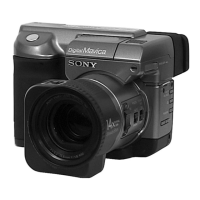
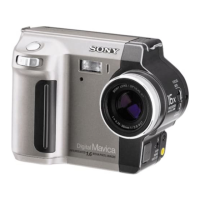
MVC-CD200/CD300
Pattern box
Front of the lens
About 34cm (MVC-CD200
About 28cm (MVC-CD300
 Loading...