6-3. Description of High-level Instructions
High-level Instruction Reference
6-3. Description of High-level Instructions
157
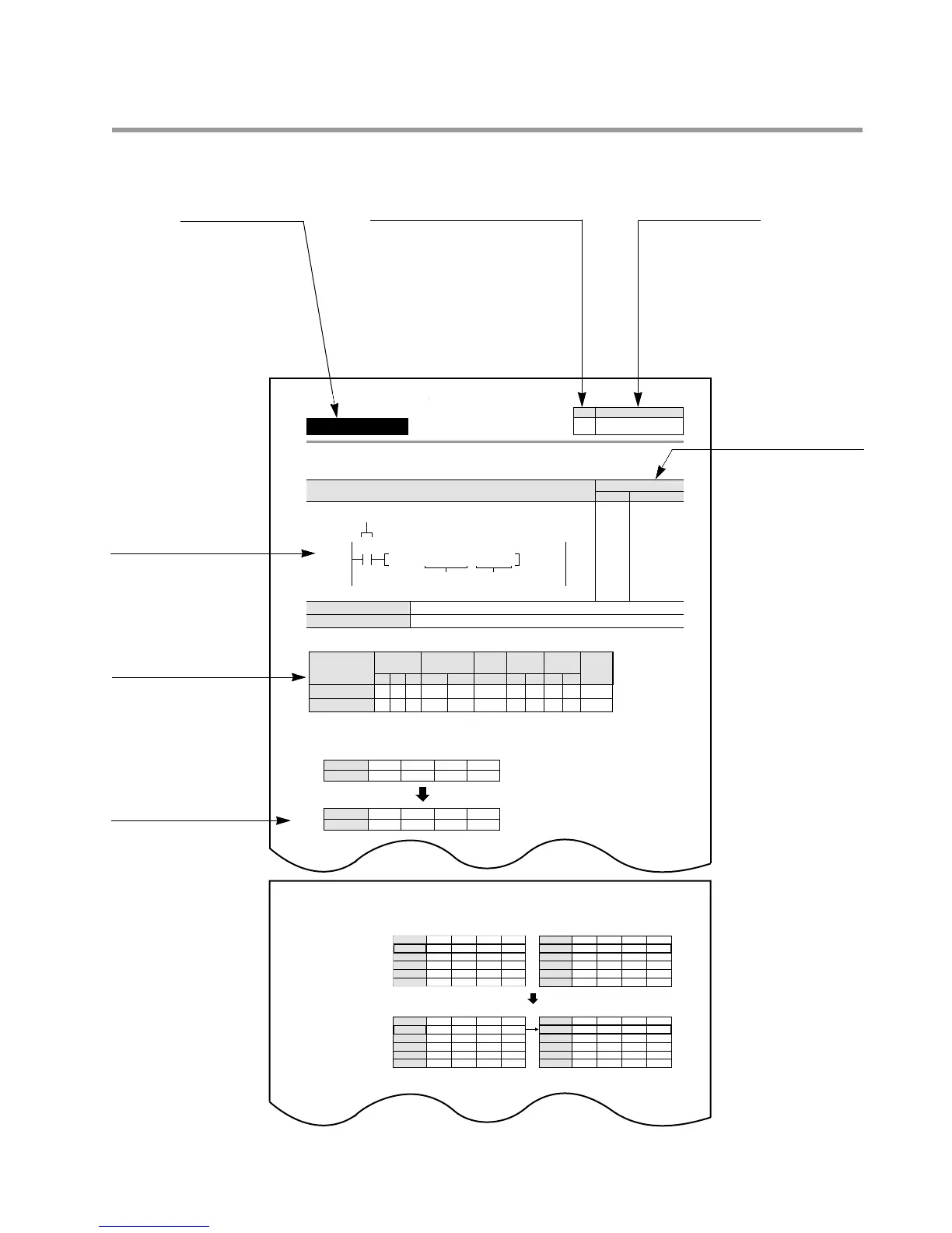
Instruction number
Ladder diagram on
the screen using
NPST-GR Software
Available operands
for instruction
Explanation of
program example,
details of instruction,
and flag conditions
Number of steps for instructions
Available unit type
Description
• The 16-bit data or 16-bit equivalent constant specified by S is copied to the area specified by D
when the trigger turns ON.
Bit position
WX0
WX1
WX2
WX3
WX4
11 8
1010
1100 1010
1110
30
Source
Trigger X0: ON
15 ••12 •• ••
74
••
0000
0000 0000
0010
0000
0000 0000
0011
0000
0000 0000
0100
0000
0000 0000
0101
[S]
Bit position
WR0
WR1
WR2
WR3
WR4
11 8
0000
0000 0000
1111
30
Destination
15 ••12 •• ••
74
••
0000
0000 0000
1110
0000
0000 0000
1101
0000
0000 0000
1100
0000
0000 0000
1011
[D]
Bit position
WX0
WX1
WX2
WX3
WX4
11 8
1010
1100 1010
1110
30
Source
15 ••12 •• ••
74
••
0000
0000 0000
0010
0000
0000 0000
0011
0000
0000 0000
0100
0000
0000 0000
0101
[S]
Bit position
WR0
WR1
WR2
WR3
WR4
11 8
1010
1100 1010
1110
30
Destination
15 ••12 •• ••
74
••
0000
0000 0000
1110
0000
0000 0000
1101
0000
0000 0000
1100
0000
0000 0000
1011
[D]
Boolean (non-ladder)
with NPST-GR
Software
6-3. Description of High-level Instructions
Outline Copies the 16-bit data to the specified 16-bit area.
Program example
■ Operands
■ Explanation of example
• The contents of word external input relay WX0 are copied to word internal relay WR0 when trigger X0 turns ON.
Timer/Counter
EV
Relay
SVWRWYWX
Operand
S
AAA A
A:
N/A: Not Available
Register
DT
A
IYIX
AA
HK
AA
Constant
Index
modifier
A
Index
register
Available
A
D
N/A A A A A A A N/A N/A AA
Bit position
WX0
1010
1100
11 8
1010
1110
30
Source [S]: HACAE
X0: ON
15 ••12 •• ••
74
••
Bit position
WR0
1010
1100
11 8
1010
1110
30
Destination [D]: HACAE
15 ••12 •• ••
74
••
F0
(MV)
16-bit data move
Availability
Step
5 All series
16-bit equivalent constant or 16-bit area (source)
16-bit area (destination)
Ladder Diagram
Boolean Non-ladder
Address Instruction
0
X0
F0 MV , WX0 , WR0
S
D
Trigger
0
1
ST X 0
F 0 (MV )
WX 0
WR 0
S
D
 Loading...