ll-bit
page
address in the
accessed
element
of
the
memory
map
array
replaces the 8
high-order
bits
of
the
virtual
ad-
dress
to
produce the
actual
address of
the
main memory
lo-
cation
to
be
used
by
the
instruction
(20-bit
word address
that
is
automatically
adjusted
as required for doubleword,
halfword, or
byte
operation).
See
Figure
7.
Note:
If
the
ll-bit
page
address in
the
accessed
element
of
the memory map
is
all
zeros,
and
an
actual
ad-
dress
is
produced
that
corresponds
to
a word address
in
the
range 0 through 15, when
the
ll-bit
page
address
is
combined with the 9 low-order bits
of
the
virtual
address,
the
corresponding
general
register
in
the
current
register
block
is
not
accessed.
In
this
one
particular
instance a word address in
the
range 0 through
15
corresponds to
an
actual
main
memory
location
rather
than a
general
register.
REAL
MEMORY
WRITE
LOCKS
Additional
memory
protection,
independent
of
the access
protection,
is
provided by a
write
lock
and
key
technique.
A
4-bit
write
protect
lock
(WL)
is
provided for
each
512-
word
page
of
actual
memory. Thus, for
the
maximum
lM-
word real memory there would
be
2048
4-bit
write
locks.
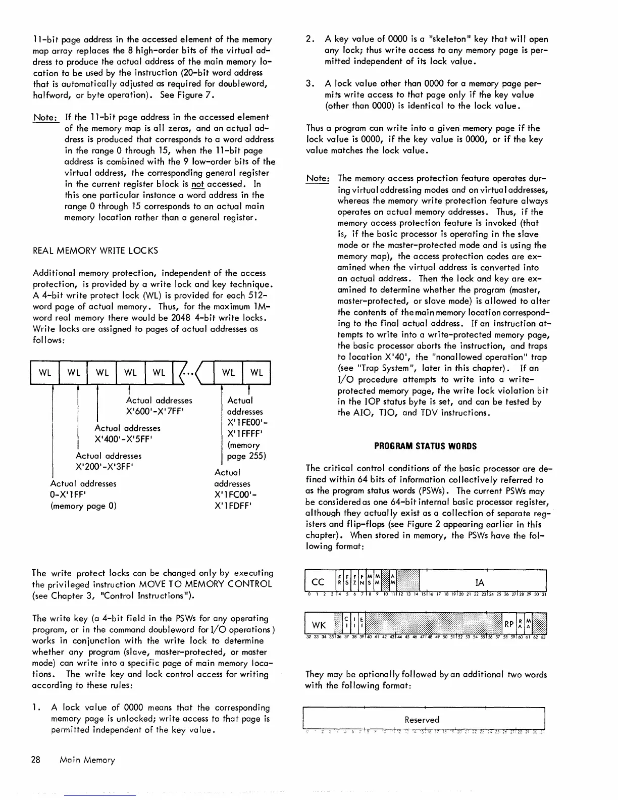
Write
locks
are
assigned to pages
of
actual
addresses as
follows:
Actual addresses
X'600'-X'7FF'
Actual addresses
X'400'-X'5FF'
Actual addresses
X'200'-X'3FF'
Actual addresses
O-X'lFF'
(memory
page
0)
Actual
addresses
X'l
FEOO'-
X'l
FFFF'
(memory
page 255)
Actual
addresses
X'lFCOO'-
X'lFDFF'
The write
protect
locks can be changed
only
by
executing
the
privileged
instruction MOVE
TO
MEMORY CONTROL
(see
Chapter
3,
"Control Instructions").
The
write
key (a
4-bit
field in the
PSWs
for
any
operating
program, or in the command doubleword for
I/O
operations)
works in
conjunction
with the
write
lock to determine
whether
any
program (slave,
master-protected,
or master
mode)
can
write
into a
specific
page of main memory
ioca-
tions.
The
write
key
and
lock control
access
for writing
according
to these rules:
1. A lock
value
of 0000 means
that
the
corresponding
memory
page
is
unlocked;
write
access
to
that
page
is
permitted
independent
of
the key
value.
28
Main
Memory
2.
A key
value
of
0000
is
a
"skeleton"
key
that
will open
any
lock; thus
write
access
to
any
memory
page
is
per-
mitted
independent
of its lock
value.
3.
A lock
value
other
than 0000 for a memory
page
per-
mits
write
access
to
that
page
only
if
the key
value
(other than 0000)
is
identical
to the lock
value.
Thus a program
can
write
into a
given
memory
page
if
the
lock
value
is
0000,
if
the
key
value
is
0000, or
if
the key
value
matches
the
lock
value.
Note:
The memory
access
protection
feature
operates
dur-
ing virtua I addressing modes
and
on virtua I addresses,
whereas
the
memory
write
protection
feature always
operates
on
actual
memory addresses. Thus,
if
the
memory
access
protection
feature
is
invoked
(that
is, if
the
basic processor
is
operating
in
the
slave
mode or the
master-protected
mode
and
is
using
the
memory map),
the
access
protection
codes
are
ex-
amined when the
virtual
address
is
converted
into
an
actual
address.
Then
the
lock and key
are
ex-
amined to
determine
whether
the program (master,
master-protected,
or
slave
mode)
is
allowed
to
alter
the
contents
of
themainmemory
location
correspond-
ing to the final
actual
address.
If
an
instruction
at-
tempts to
write
into a
write-protected
memory
page,
the
basic processor aborts
the
instruction,
and
traps
to
location
X
'40',
the
"nonallowed
operation"
trap
(see
"Trap System ",
later
in this
chapter).
If
an
I/O
procedure attempts to
write
into
a
write-
protected
memory
page,
the
write
lock
violation
bit
in
the
lOP
status
byte
is
set,
and can
be
tested
by
the
AIO,
no,
and
TDV
instructions.
PROGRAM
STATUS
WORDS
The
critical
control conditions
of
the basic processor
are
de-
fined
within
64
bits
of
information
collectively
referred to
as
the
program status words (PSWs). The
current
PSWs
may
be
considered as
one
64-bit
internal
basic
processor register,
although
they
actually
exist
as a
collection
of
separate
n~g
isters
and
flip-flops
(see Figure 2
appearing
earlier
in this
chapter).
When stored in memory,
the
PSWs
have
the
fol-
lowing format:
They may
be
optionally
followed
byan
additional
two words
with the following format:
.:,
 Loading...