KC705 Evaluation Board 10
UG810 (v1.8) March 20, 2018 www.xilinx.com
Chapter 1: KC705 Evaluation Board Features
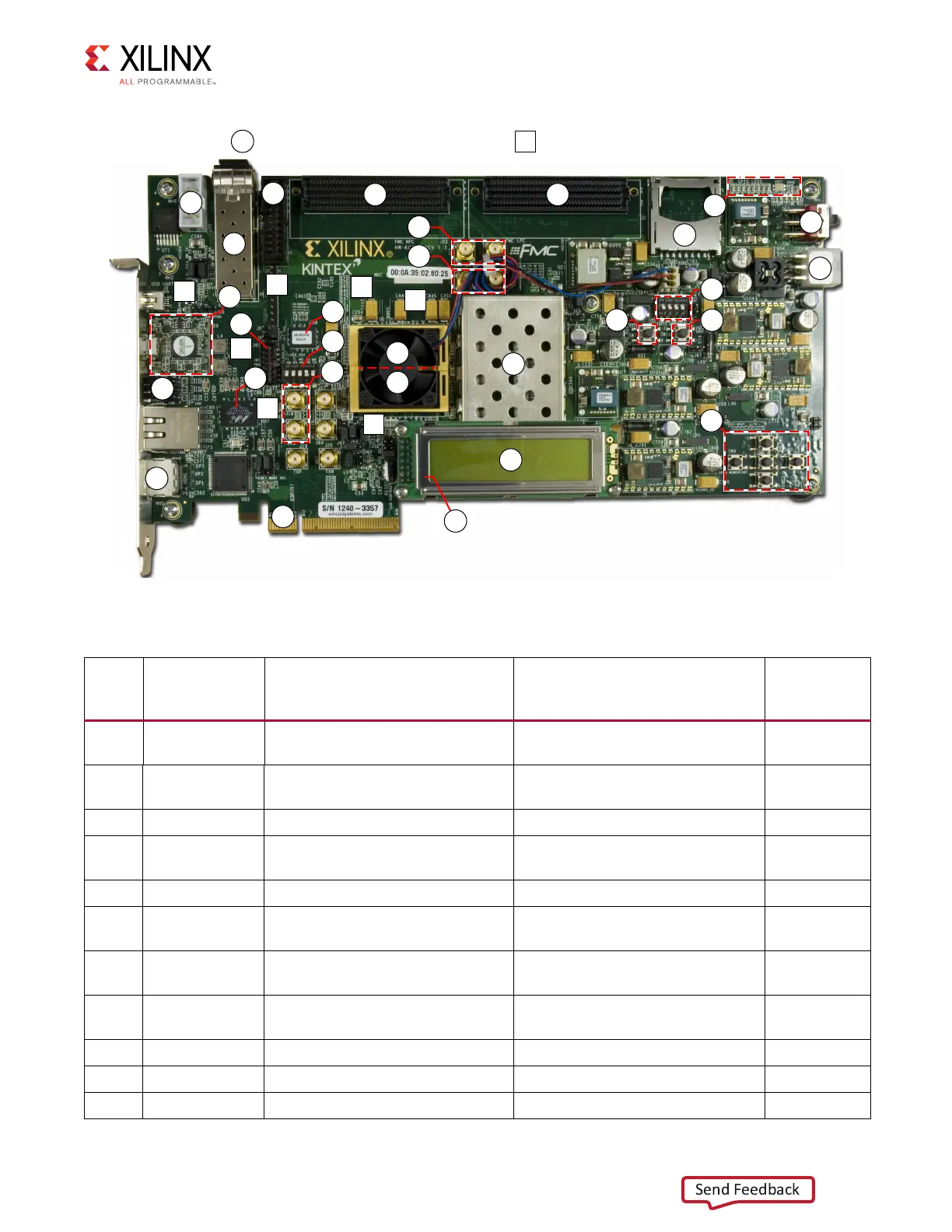
X-Ref Target - Fig ure 1-2
Figure 1-2: KC705 Board Components
UG841_c1_02_042313
3
30
31
33
14
17
21
4
29
1
8
7
12
15
10
11
18
6
13
16
2
26
9
00
Square callout references a component
on the back side of the board
Round callout references a component
on the front side of the board
00
5
27
19
28
22
24
23
User rotary switch
located under LCD
25
20
35
36
34
37
Table 1-1: KC705 Board Component Descriptions
Callout
Reference
Designator
Component Description Notes
Schematic
0381397
Page Number
1U1Kintex-7 FPGA (Located under
fansink)
XC7K325T-2FFG900C, Radian
INC3001-7_1.5BU_LI98
2J1DDR3 Memory Module, under EMI
shield
Micron MT8JTF12864HZ-1G6G1 15
3U58Linear BPI Flash Memory Micron PC28F00AP30TF 26
4U7Quad SPI Flash Memory Micron N25Q128A13BSF40F or
Micron MT25QL128ABA8ESF-0SIT
26
5U9SD Card Interface Molex 67840-8001 28
6 USB JTAG Module Digilent USB JTAG Module (with
micro-B receptacle)
14
7U6System Clock Source (back side of
board)
SiTime SIT9102-243N25E200.0000 23
8U45Programmable User Clock Source
(back side of board)
Silicon Labs SI570BAB0000544DG 23
9 J11, J12 User SMA Clock Input Rosenberger 32K10K-400L5 23
10 J15, J16 GTX SMA Clock Input Rosenberger 32K10K-400L5 23
11 U70 Jitter Attenuated Clock Silicon Labs SI5324C-C-GM 24
 Loading...


