KC705 Evaluation Board 84
UG810 (v1.8) March 20, 2018 www.xilinx.com
Appendix A: Default Switch and Jumper Settings
DIP Switch SW13 Mode and Flash Memory Address
Settings
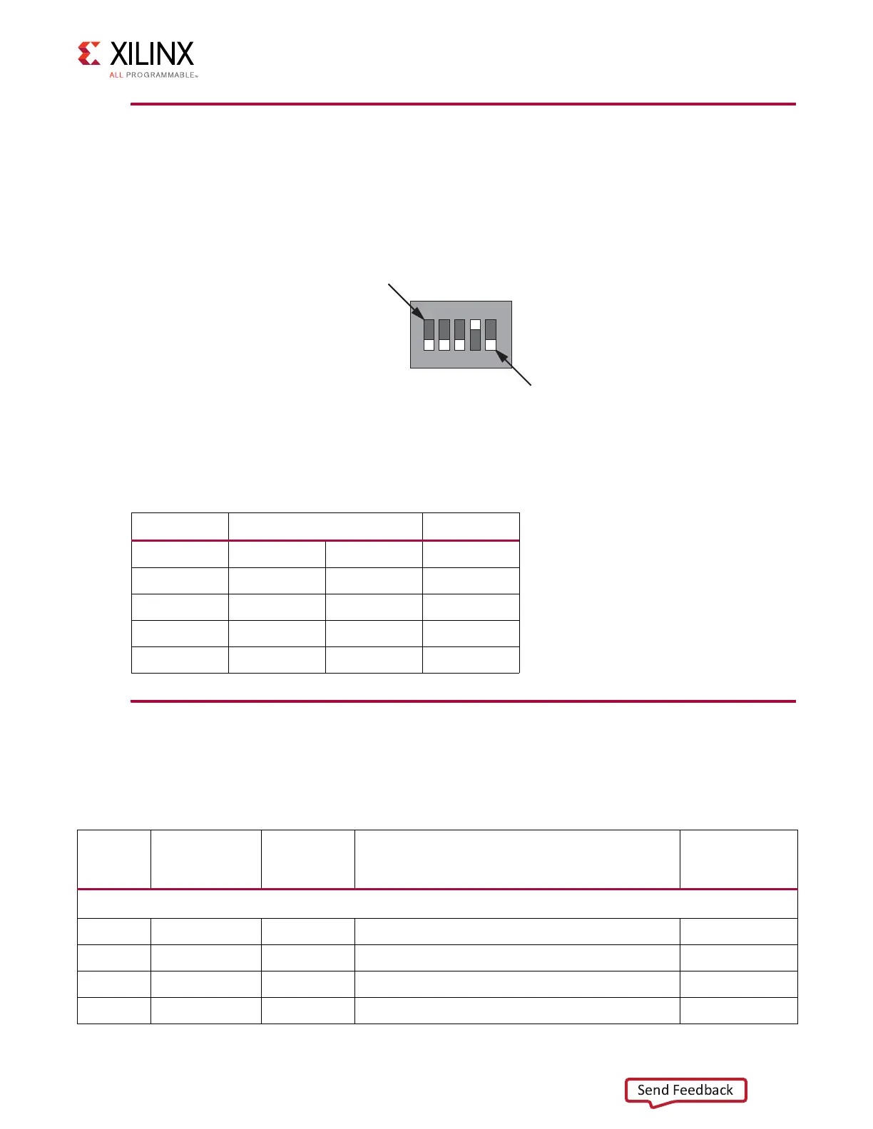
See Figure 1-2, page 10 Item 29 for location of SW13. Default settings are shown in
Figure A-2 and details are listed in Table A-2.
The default mode setting M[2:0] = 010 selects Master BPI configuration at board power-on.
Default Jumper Settings
See Figure A-3 for the locations of jumpers listed in Table A-3.
X-Ref Target - Figure A-2
Figure A-2: SW13 Default Settings
Table A-2: SW13 Default Switch Settings
Position Function Default
1FLASH_A25A25 Off
2FLASH_A24A24 Off
3FPGA_M2M2 Off
4FPGA_M1M1 On
5FPGA_M0M0 Off
UG810_aA_02_031214
1
SW13
OFF Position = 0
ON Position = 1
2345
A25
A24
M2
M1
M0
Table A-3: KC705 Default Jumper Settings
Callout
Header
Reference
Designator
Jumper
Position
Description
Schematic
0381502 Page
2-pin
1 J3 1-2 SPI SELECT = Onboard SPI flash memory device 26
2 J42 None U35 REF3012 XADC_AGND L17 bypassed 31
3 J43 1-2 U35 REF3012 XADC_AGND = GND 31
4 J53 None U55 UCD9248 RESET_B = LOGIC 1 (NOT RESET) 36
 Loading...


