KC705 Evaluation Board 13
UG810 (v1.8) March 20, 2018 www.xilinx.com
Chapter 1: KC705 Evaluation Board Features
For full details on configuring the FPGA, see 7 Series FPGAs Configuration User Guide
(UG470) [Ref 2].
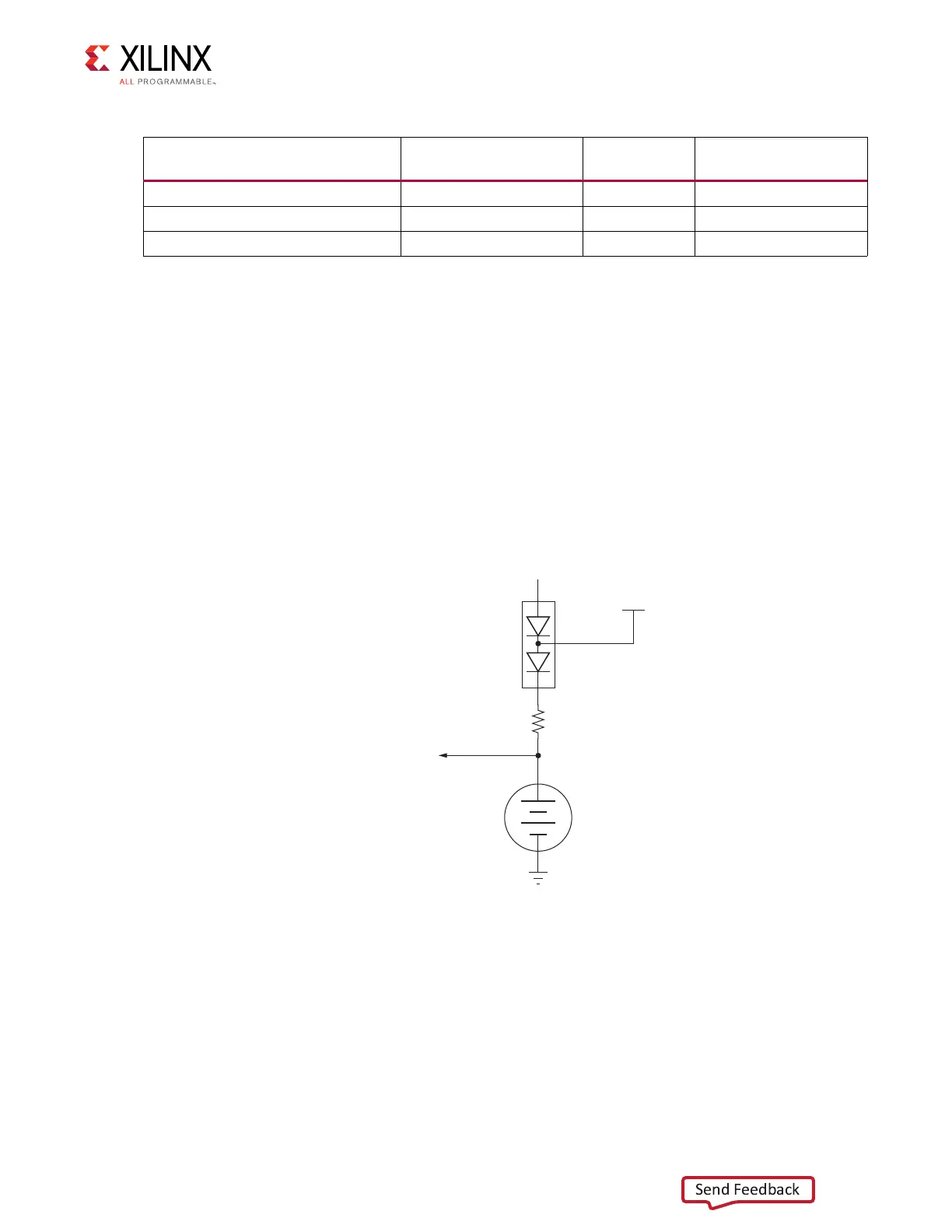
Encryption Key Backup Circuit
FPGA U1 implements bitstream encryption key technology. The KC705 board provides the
encryption key backup battery circuit shown in Figure 1-4. The rechargeable 1.5V lithium
button-type battery B1 is soldered to the board with the positive output connected to FPGA
U1 VCCBATT pin C10. The battery supply current I
BATT
specification is 150 nA max when
board power is off. B1 is charged from the VCCAUX_IO 2.0V rail through a series diode with
a typical forward voltage drop of 0.38V. and 4.7 KΩ current limit resistor. The nominal
charging voltage is 1.62V.
I/O Voltage Rails
There are 10 I/O banks available on the Kintex-7 device. The voltages applied to the FPGA
I/O banks used by the KC705 board are listed in Table 1-3.
Table 1-2: KC705 Board FPGA Configuration Modes
Configuration Mode
SW13 DIP Switch
Settings (M[2:0])
Bus Width CCLK Direction
Master SPI 001 x1, x2, x4 Output
Master BPI 010 x8, x16 Output
JTAG 101 x1 Not applicable
X-Ref Target - Figure 1-4
Figure 1-4: Encryption Key Backup Circuit
UG810_c1_04_031214
GND
2
1
B1
Lithium Battery
Seiko
TS518SE_FL35E
2
1
3
BAS40-04
D11
40V
200 mW
NC
FPGA_VBATT
+
VCCAUX_IO (2.0V)
R406
4.70K 1%
1/16W
To FPGA U1 Pin C10
(VCCBATT)
 Loading...


