KC705 Evaluation Board 35
UG810 (v1.8) March 20, 2018 www.xilinx.com
Chapter 1: KC705 Evaluation Board Features
For more information on the GTX transceivers, see 7 Series FPGAs GTX Transceivers
User Guide (UG476) [Ref 12].
PCI Express Edge Connector
[Figure 1-2, callout 13]
The 8-lane PCI Express edge connector performs data transfers at the rate of 2.5 GT/s for a
Gen1 application and 5.0 GT/s for a Gen2 application. The PCIe transmit and receive signal
datapaths have a characteristic impedance of 85Ω ±10%. The PCIe clock is routed as a 100Ω
differential pair. The 7 series FPGAs GTX transceivers are used for multi-gigabit per second
serial interfaces.
The XC7K325T-2FFG900C FPGA (-2 speed grade) included with the KC705 board supports
up to Gen2 x8.
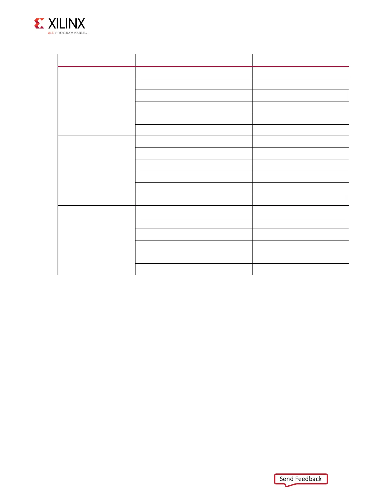
MGT_BANK_116 GTXE2_CHANNEL_X0Y4 PCIe3
GTXE2_CHANNEL_X0Y5 PCIe2
GTXE2_CHANNEL_X0Y6 PCIe1
GTXE2_CHANNEL_X0Y7 PCIe0
MGTREFCLK0 Si5326
MGTREFCLK1 FMC LPC GBT_CLK0
MGT_BANK_117 GTXE2_CHANNEL_X0Y8 SMA
GTXE2_CHANNEL_X0Y9 SGMII
GTXE2_CHANNEL_X0Y10 SFP+
GTXE2_CHANNEL_X0Y11 FMC LPC DP0
MGTREFCLK0 SGMII_CLK
MGTREFCLK1 SMA_CLK
MGT_BANK_118 GTXE2_CHANNEL_X0Y12 FMC HPC DP0
GTXE2_CHANNEL_X0Y13 FMC HPC DP1
GTXE2_CHANNEL_X0Y14 FMC HPC DP2
GTXE2_CHANNEL_X0Y15 FMC HPC DP3
MGTREFCLK0 FMC HPC GBT_CLK0
MGTREFCLK1 FMC HPC GBT_CLK1
Table 1-10: GTX Interface Connections for FPGA U1 (Cont’d)
Transceiver Bank Associated Net Name Connections
 Loading...


