KC705 Evaluation Board 85
UG810 (v1.8) March 20, 2018 www.xilinx.com
Appendix A: Default Switch and Jumper Settings
5 J56 None U56 UCD9248 RESET_B = LOGIC 1 (NOT RESET) 40
6 J65 1-2 FMC VADJ = ON 36
7 J68 1-2 XADC_VCC5V0 =VCC5V0 (5V) 31
3-pin
8 J27 2-3 SFP RX BW = FULL 22
9 J28 2-3 SFP TX BW = FULL 22
10 J29 1-2 U32 EPHY CONFIG5 = LOGIC 1 25
11 J30 1-2 U32 EPHY CONFIG4 = LOGIC 1 25
12 J47 1-2 XADC_VREFP = REF3012 XADC_VREF 31
13 J48 2-3 XADC_VCC = ADP123 1.85V 31
14 J69 1-2 REF3012 VIN = XADC_VCC5V0 31
2x3
15 J32 5-6 PCIe lane width = 8 21
Table A-3: KC705 Default Jumper Settings (Cont’d)
Callout
Header
Reference
Designator
Jumper
Position
Description
Schematic
0381502 Page
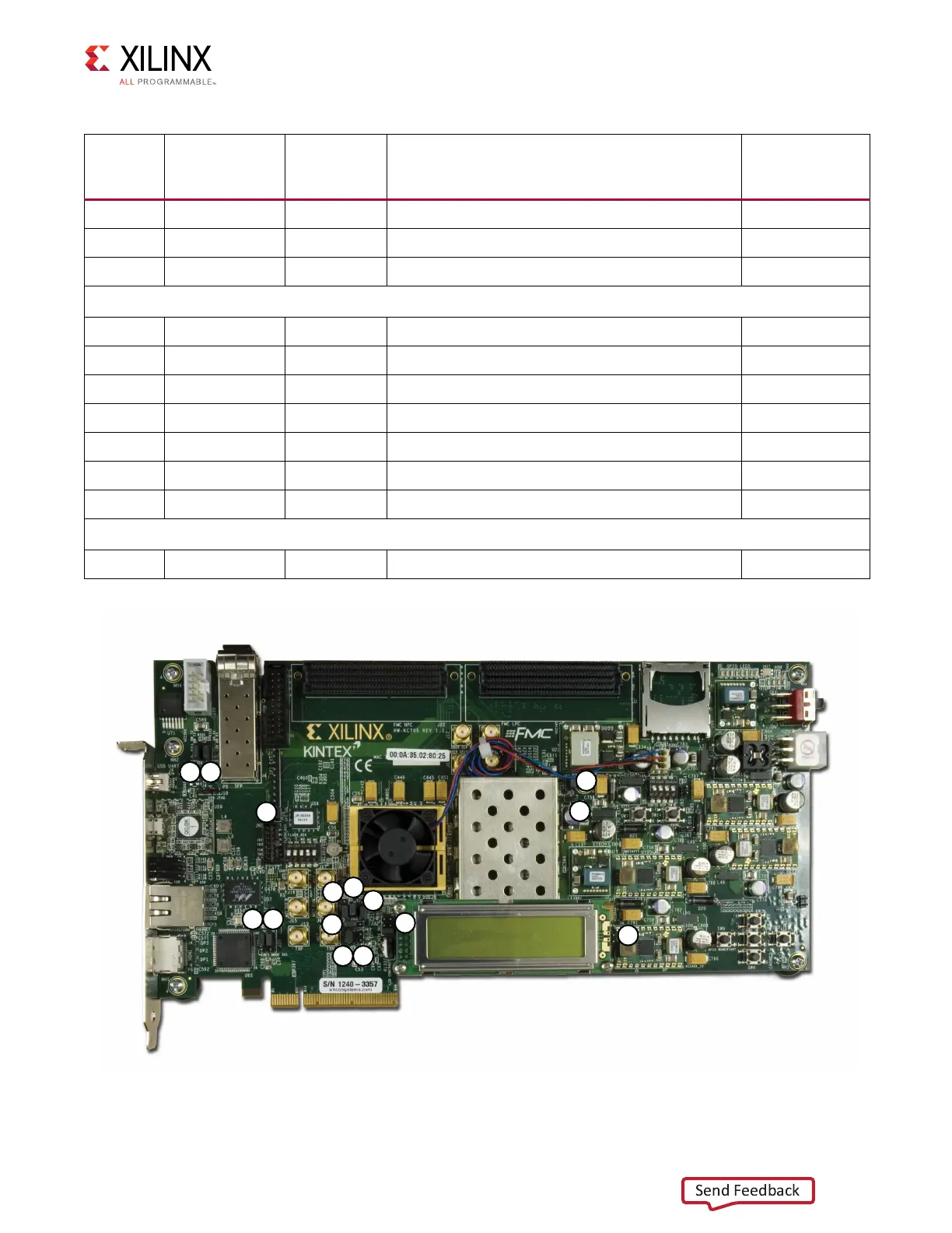
X-Ref Target - Figure A-3
Figure A-3: KC705 Jumper Locations
1
2
15
5
4
6
14
7
13
12
1110
8
9
3
UG810_aA_03_111414
 Loading...


