KC705 Evaluation Board 9
UG810 (v1.8) March 20, 2018 www.xilinx.com
Chapter 1: KC705 Evaluation Board Features
Feature Descriptions
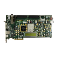
Figure 1-2 shows the KC705 board. Each numbered feature that is referenced in Figure 1-2
is described in the sections that follow.
Note:
The image in Figure 1-2 is for reference only and might not reflect the current revision of the
board.
X-Ref Target - Fig ure 1-1
Figure 1-1: KC705 Board Block Diagram
UG810_c1_01_011812
Kintex-7 FPGA
XC7K325T-2FFG900C
128 MB Linear BPI
Flash memory
128 Mb Quad-SPI
Flash Memory
8-lane PCI Express
Edge Connector
LCD Display
(2 line x 16 characters)
1 KB EEPROM (I
2
C)
I
2
C Bus Switch
XADC Header
User Switches,
Buttons, and LEDs
HDMI Video
Interface
Differential Clock
GTX SMA Clock
1 GB DDR3 Memory
(SODIMM)
FMC Connectors
(HPC/LPC)
10/100/1000 Ethernet
Interface
DIP Switch SW13
Config and Flash Addr
USB-to-UART Bridge
JTAG Interface
mini-B USB Connector
SFP+ Single Cage
 Loading...


