KC705 Evaluation Board 29
UG810 (v1.8) March 20, 2018 www.xilinx.com
Chapter 1: KC705 Evaluation Board Features
System Clock Source
[Figure 1-2, callout 7]
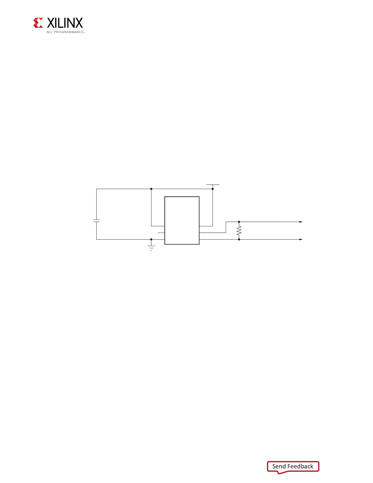
The KC705 board has a 2.5V LVDS differential 200 MHz oscillator (U6) soldered onto the
back side of the board and wired to an FPGA MRCC clock input on bank 33. This 200 MHz
signal pair is named SYSCLK_P and SYSCLK_N, which are connected to FPGA U1 pins AD12
and AD11 respectively.
• Oscillator: Si Time SiT9102AI-243N25E200.00000 (200 MHz)
• PPM frequency jitter: 50 ppm
• Differential Output
The system clock circuit is shown in Figure 1-10.
For more about the Si Time SiT9102 see [Ref 6].
Programmable User Clock Source
[Figure 1-2, callout 8]
The KC705 board has a programmable low-jitter 3.3V differential oscillator (U45) the FPGA
MRCC inputs of bank 15. This USER_CLOCK_P and USER_CLOCK_N clock signal pair are
connected to FPGA U1 pins K28 and K29 respectively. On power-up the user clock defaults
to an output frequency of 156.250 MHz. User applications can change the output frequency
within the range of 10 MHz to 810 MHz through an I2C interface. Power cycling the KC705
board reverts the user clock to its default frequency of 156.250 MHz.
• Programmable Oscillator: Silicon Labs Si570BAB0000544DG (10 MHz - 810 MHz)
• Differential Output
• I2C address 0x5D
X-Ref Target - Figure 1-10
Figure 1-10: System Clock Source
UG810_c1_10_031214
GND
VCC2V5
SIT9102
200 MHz
Oscillator
OE
NC
GND
VCC
OUT_B
OUT
1
2
3
6
5
4
U6
R459
100Ω 1%
SYSCLK_P
SYSCLK_N
C550
0.1 μF 10V
X5R
 Loading...


