KC705 Evaluation Board 24
UG810 (v1.8) March 20, 2018 www.xilinx.com
Chapter 1: KC705 Evaluation Board Features
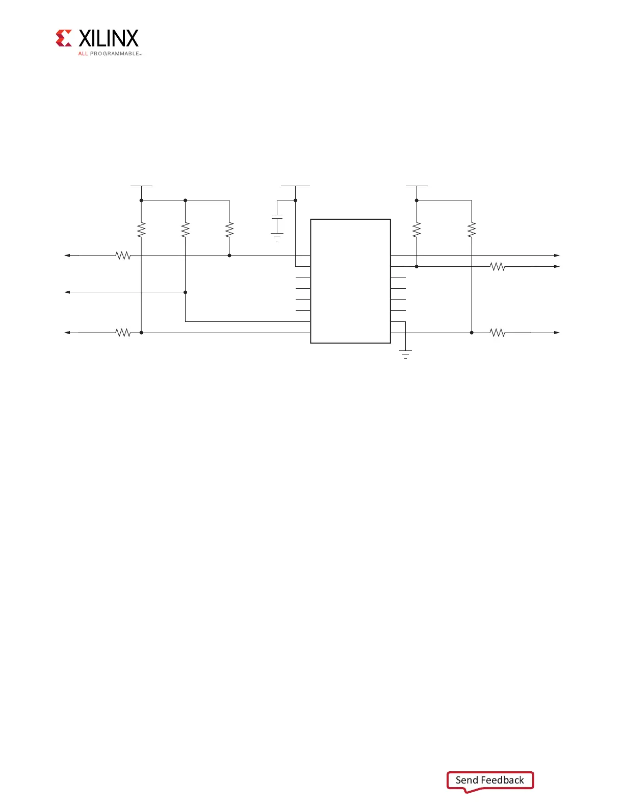
The configuration section of7 Series FPGAs Configuration User Guide (UG470) [Ref 2]
provides details on using the Quad SPI flash memory. Figure 1-6 shows the connections of
the Quad SPI flash memory on the KC705 board.
For more information about the Micron N25Q128A13BSF40F or MT25QL128ABA8ESF-0SIT
parts, see [Ref 5].
SD Card Interface
[Figure 1-2, callout 5]
The KC705 board includes a secure digital input/output (SDIO) interface to provide
user-logic access to general purpose nonvolatile SDIO memory cards and peripherals. The
SD card slot is designed to support 50 MHz high speed SD cards.
The SDIO signals are connected to I/O bank 12 which has its VCCO set to VADJ. A Texas
Instruments I TXB0108 8-bit bidirectional voltage-level translator is used between the FPGA
X-Ref Target - Fig ure 1-6
Figure 1-6: 128 Mb Quad SPI Flash Memory
UG810_c1_06_031214
VCC2V5
N25Q128
128 Mb Serial
Flash Memory
GND
1
2
3
5
7
6
U7
4
8
VCC_SPI
C18
0.1μF 25V
X5R
FLASH_D2
DQ1
16
15
14
12
10
11
13
9
SB
NC3
NC2
NC1
NC0
VCC
HOLD_B/DQ3
WB/VPP/DQ2
VSS
NC4
NC5
NC6
NC7
DQ0
C
R17
DNP
R18
4.7kΩ 5%
R431
15Ω 1%
R432
15Ω 1%
FLASH_D0
FPGA_CCLK
FLASH_D2_R
FLASH_D0_R
GND
VCC2V5
R20
DNP
R19
4.7kΩ 5%
R21
4.7kΩ 5%
R430
15Ω 1%
R429
15Ω 1%
FLASH_D2_R
FLASH_D3_R
FLASH_D3
FLASH_D1
QSPI_IC_CS_B
 Loading...


