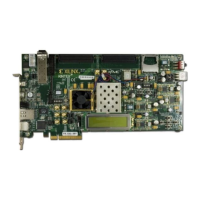
KC705 Evaluation Board 23
UG810 (v1.8) March 20, 2018 www.xilinx.com
Chapter 1: KC705 Evaluation Board Features
Quad SPI Flash Memory
[Figure 1-2, callout 4]
The Quad SPI flash memory located at U7 on the back side of the board provides 128 Mb of
nonvolatile storage that can be used for configuration and data storage.
• Part number: Micron N25Q128A13BSF40F or MT25QL128ABA8ESF-0SIT
• Supply voltage: 2.8V
• Datapath width: 4 bits
• Data rate: Various depending on Single/Dual/Quad mode and CCLK rate
Four data lines and the FPGA CCLK pin are wired to the Quad SPI flash memory. A common
chip select (FPGA_FCS) shared between the Linear BPI flash memory and the Quad SPI flash
memory is controlled by the configuration mode settings on DIP switch SW13 position 5
(M0) and a one-of-two demultiplexer device U64. If mode pin M0 = 1, the SPI flash memory
device is selected. If mode pin M0 = 0, the Linear BPI flash memory device is selected. The
connections between the SPI flash memory and the FPGA are listed in Table 1-6.
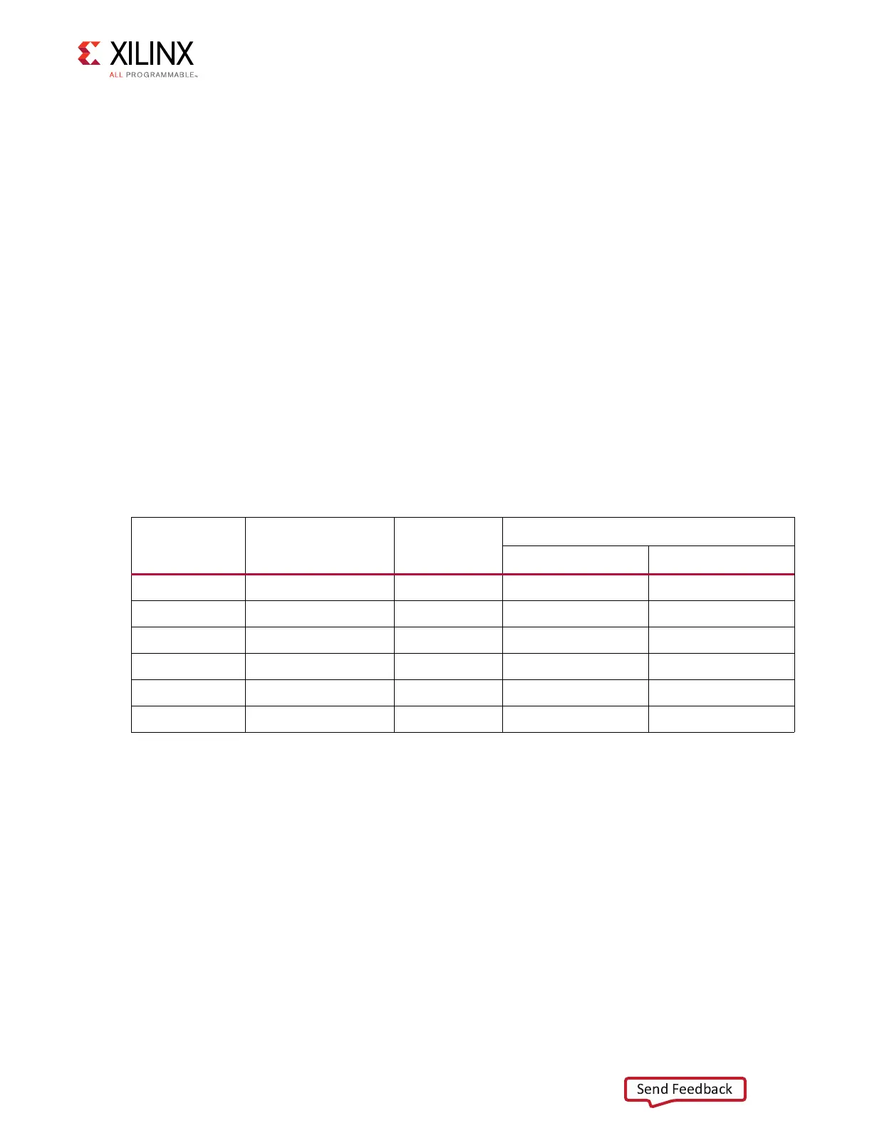
Table 1-6: Quad SPI Flash Memory Connections to the FPGA
U1 FPGA Pin Net Name I/O Standard
J1 DDR3 Memory
Pin Number Pin Name
P24 FLASH_D0 LVCMOS25 15 DQ0
R25 FLASH_D1 LVCMOS25 8 DQ1
R20 FLASH_D2 LVCMOS25 9 DQ2
R21 FLASH_D3 LVCMOS25 1 DQ3
B10 FPGA_CCLK N/A 16 C
U19 QSPI_IC_CS_B
(1)
LVCMOS25 7 S_B
Notes:
1. FPGA_FCS connected to FPGA U1 pin U19 becomes QSPI_IC_CS_B through U64 and J3.
 Loading...


