KC705 Evaluation Board 36
UG810 (v1.8) March 20, 2018 www.xilinx.com
Chapter 1: KC705 Evaluation Board Features
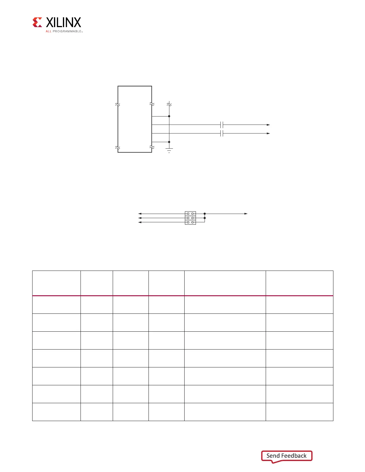
The PCIe clock is input from the edge connector. It is AC coupled to the FPGA through the
MGTREFCLK1 pins of Quad 115. PCIE_CLK_Q0_P is connected to FPGA U1 pin U8, and the _N
net is connected to pin U7. The PCI Express clock circuit is shown in Figure 1-15.
PCIe lane width/size is selected via jumper J32 (Figure 1-16). The default lane size selection
is 8-lane (J32 pins 5 and 6 jumpered).
Table 1-11 lists the PCIe edge connector connections.
X-Ref Target - Figure 1-15
Figure 1-15: PCI Express Clock
X-Ref Target - Figure 1-16
Figure 1-16: PCI Express Lane Size Select Jumper J32
UG810_c1_15_031214
PCI Express
Eight-Lane
Edge connector
GND
GND
A15
A13
A14
P1
REFCLK+
A12
GND
C544
0.01μF 25V
X7R
C545
0.01μF 25V
X7R
PCIE_CLK_Q0_P
PCIE_CLK_Q0_N
PCIE_CLK_Q0_C_P
PCIE_CLK_Q0_C_N
OE
REFCLK-
UG810_c1_16_031214
PCIE_PRSNT_B
PCIE_PRSNT_X1
PCIE_PRSNT_X4
PCIE_PRSNT_X8
J32
1
3
5
2
4
6
Table 1-11: PCIe Edge Connector Connections
Schematic Net
Name
FPGA Pin
(U1)
PCIe Edge
Connector
Pin
PCIe Edge
Pin Name
Function FFG900 Placement
PCIE_RX0_P M6 B14 PETp0 Integrated Endpoint block
receive pair
GTXE2_CHANNEL_X0Y7
PCIE_RX0_N M5 B15 PETn0 Integrated Endpoint block
receive pair
GTXE2_CHANNEL_X0Y7
PCIE_RX1_P P6 B19 PETp1 Integrated Endpoint block
receive pair
GTXE2_CHANNEL_X0Y6
PCIE_RX1_N P5 B20 PETn1 Integrated Endpoint block
receive pair
GTXE2_CHANNEL_X0Y6
PCIE_RX2_P R4 B23 PETp2 Integrated Endpoint block
receive pair
GTXE2_CHANNEL_X0Y5
PCIE_RX2_N R3 B24 PETn2 Integrated Endpoint block
receive pair
GTXE2_CHANNEL_X0Y5
PCIE_RX3_P T6 B27 PETp3 Integrated Endpoint block
receive pair
GTXE2_CHANNEL_X0Y4
 Loading...


