KC705 Evaluation Board 81
UG810 (v1.8) March 20, 2018 www.xilinx.com
Chapter 1: KC705 Evaluation Board Features
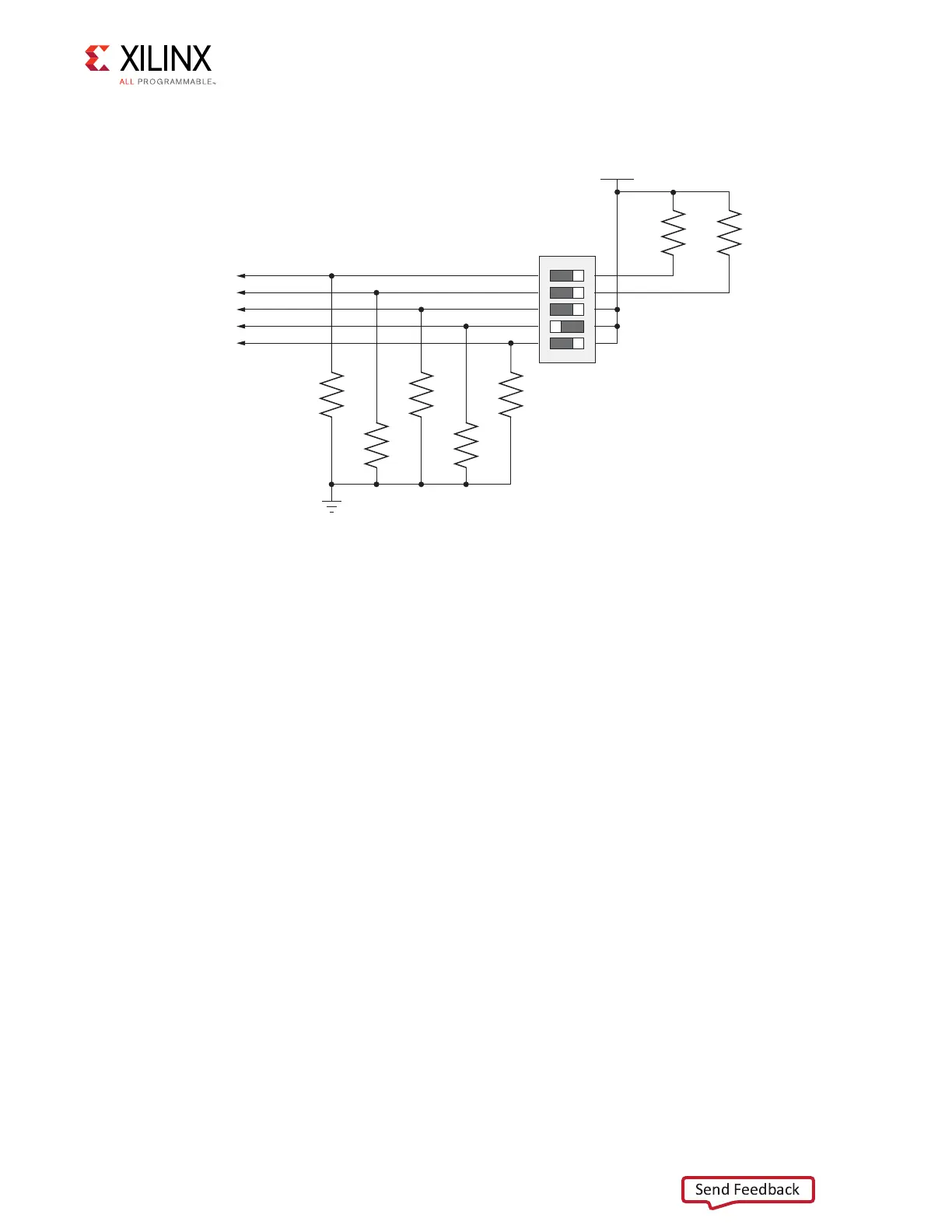
Figure 1-39 shows mode switch SW13.
The mode pins settings on SW13 determine if the Linear BPI or the Quad SPI flash memory
is used for configuring the FPGA. DIP switch SW13 also provides the upper two address bits
for the Linear BPI flash memory and can be used to select one of multiple stored
configuration bitstreams. Figure 1-40 shows the connectivity between the onboard
nonvolatile flash devices used for configuration and the FPGA.
To obtain the fastest configuration speed an external 66 MHz oscillator is wired to the
EMCCLK pin of the FPGA. This allows users to create bitstreams that configure the FPGA
over the 16-bit datapath from the Linear BPI flash memory at a maximum synchronous read
rate of 33 MHz. The bitstream stored in the flash memory must be generated with a BitGen
option to divide the EMCCLK by two.
X-Ref Target - Figure 1-39
Figure 1-39: Mode Switch
UG810_c1_39_031214
SDA05H1SBD
SW13
R401
220Ω
0.1 W
1%
R402
220Ω
0.1 W
1%
VCC2V5
FPGA_M2
FPGA_M1
FPGA_M0
FLASH_A25
FLASH_A24
R396
1.21kΩ
0.1 W
1%
R397
1.21kΩ
0.1 W
1%
R398
1.21kΩ
0.1 W
1%
R399
1.21kΩ
0.1 W
1%
R400
1.21kΩ
0.1 W
1%
1
2
3
4
5
10
9
8
7
6
GND
ON
 Loading...


