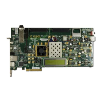
KC705 Evaluation Board 80
UG810 (v1.8) March 20, 2018 www.xilinx.com
Chapter 1: KC705 Evaluation Board Features
Configuration Options
The FPGA on the KC705 board can be configured by the following methods:
• Master BPI (uses the Linear BPI flash memory)
• Master SPI (uses the Quad SPI flash memory)
• JTAG (uses the USB-to-JTAG Bridge or Download cable). See USB JTAG Module, page 26
for more information
See 7 Series FPGAs Configuration User Guide (UG470) [Ref 2] for details on configuration
modes.
The method used to configure the FPGA is controlled by the mode pin (M2, M1, M0)
settings selected through DIP switch SW13. Table 1-35 lists the supported mode switch
settings.
GND 16 Digital Ground (board) Reference
XADC_GPIO_3, 2, 1, 0 19, 20, 17, 18 Digital I/O. These pins should come from the same bank. These I/Os
should not be shared with other functions because they are required to
support 3-state operation.
Table 1-34: XADC Header J46 Pinout (Cont’d)
Net Name
J46 Pin
Number
Description
Table 1-35: Mode Switch SW13 Settings
Configuration Mode Mode Pins (M[2:0]) Bus Width CCLK Direction
Master SPI 001 x1, x2, x4 Output
Master BPI 010 x8, x16 Output
JTAG 101 x1 Not Applicable
 Loading...


