KC705 Evaluation Board 62
UG810 (v1.8) March 20, 2018 www.xilinx.com
Chapter 1: KC705 Evaluation Board Features
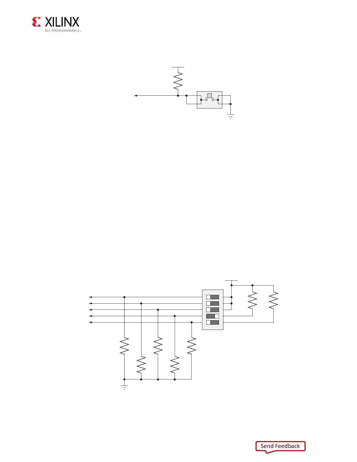
Figure 1-33 shows SW14.
Configuration Mode and Upper Linear Flash Address Switch (SW13)
[Figure 1-2, callout 29]
FPGA Configuration Mode: DIP switch SW13 positions 3, 4, and 5 control which
configuration mode is used at power-up or when the PROG pushbutton is pressed.
Linear BPI Flash Memory Upper Addresses: DIP switch SW13 positions 1 and 2 control the
setting of address bits FLASH_A25 and FLASH_A24. The mode signals FPGA_M2, _M1 and
_M0 are connected to FPGA U1 pins AB1, AB2 and AB5 respectively. The BPI flash memory
U58 address signals FLASH_A24 AND FLASH_A25 are connected to FPGA U1 pins M23 and
M22 respectively. Configuration mode is used at power-up or when the PROG pushbutton
is pressed.
Figure 1-34 shows the SW13 circuit.
X-Ref Target - Figure 1-33
Figure 1-33: FPGA_PROG_B Pushbutton SW14
X-Ref Target - Figure 1-34
Figure 1-34: Configuration Mode and Upper Linear Flash Address Switch
UG810_c1_33_031214
VCC2V5
FPGA_PROG_B
R295
4.7kΩ
0.1 W
5%
GND
1
23
4
SW14
UG810_c1_34_031214
SDA05H1SBD
SW13
R401
220Ω
0.1 W
1%
R402
220Ω
0.1 W
1%
VCC2V5
FPGA_M2
FPGA_M1
FPGA_M0
FLASH_A25
FLASH_A24
R396
1.21kΩ
0.1 W
1%
R397
1.21kΩ
0.1 W
1%
R398
1.21kΩ
0.1 W
1%
R399
1.21kΩ
0.1 W
1%
R400
1.21kΩ
0.1 W
1%
1
2
3
4
5
10
9
8
7
6
GND
 Loading...


