KC705 Evaluation Board 52
UG810 (v1.8) March 20, 2018 www.xilinx.com
Chapter 1: KC705 Evaluation Board Features
Table 1-23 lists the connections between the FPGA and the LCD header.
For more information about the Displaytech S162D LCD, see [Ref 18].
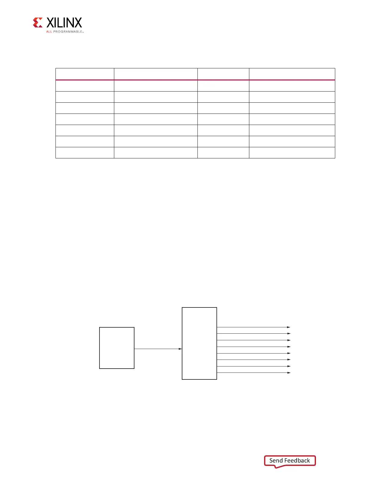
I2C Bus Switch
[Figure 1-2, callout 20]
The KC705 board implements a single I2C port on the FPGA (IIC_SDA_MAIN, IIC_SDA_SCL),
which is routed through a TI PCA9548 1-to-8 channel I2C switch (U49). U49 pin 24 net
IIC_MUX_RESET_B is connected to U1 bank 15 pin P23. This is an active-Low signal and must
be driven High (FPGA U1 pin P23) to enable I2C bus transactions between the FPGA U1 and
the other components on the I2C bus. The I2C switch can operate at speeds up to 400 kHz.
The U49 bus switch at I2C address 0x74/0b01110100 must be addressed and configured
to select the desired target back-side device.
The KC705 board I2C bus topology is shown in Figure 1-23.
User applications that communicate with devices on one of the downstream I2C buses must
first set up a path to the desired bus through the U49 bus switch at I2C address
0x74/0b01110100.
Table 1-23: FPGA to LCD Header Connections
FPGA Pin (U1) Schematic Net Name I/O Standard LCD Header Pin (J31)
AA13 LCD_DB4_LS LVCMOS15 4
AA10 LCD_DB5_LS LVCMOS15 3
AA11 LCD_DB6_LS LVCMOS15 2
Y10 LCD_DB7_LS LVCMOS15 1
AB13 LCD_RW_LS LVCMOS15 10
Y11 LCD_RS_LS LVCMOS15 11
AB10 LCD_E_LS LVCMOS15 9
X-Ref Target - Figure 1-23
Figure 1-23: I2C Bus Topology
PCA9548
1
2
C 1-to-8
Bus Switch
CH7 - SI5326_SDA/SCL
U49
IIC_SDA/SCL_MAIN
CH6 - IIC_SDA/SCL_DDR3
CH5 - IIC_SDA/SCL_HDMI
CH4 - SFP_IIC_SDA/SCL
CH3 - EEPROM_IIC_SDA/SCL
CH2 - FMC_LPC_IIC_SDA/SCL
CH1 - FMC_HPC_IIC_SDA/SCL
CH0 - USER_CLOCK_SDA/SCL
FPGA
Bank 15
(2.5V)
U1
UG810_C1_23_031214
 Loading...


