KC705 Evaluation Board 25
UG810 (v1.8) March 20, 2018 www.xilinx.com
Chapter 1: KC705 Evaluation Board Features
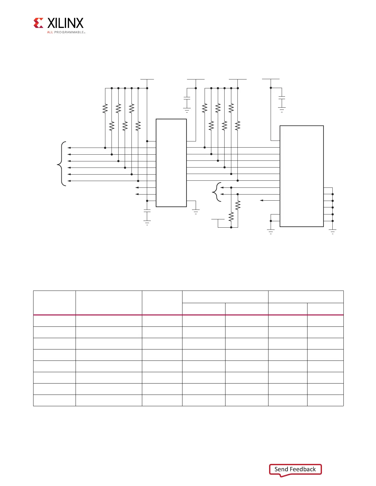
and the SD card connector (U9). Figure 1-7 shows the connections of the SD card interface
on the KC705 board.
Table 1-7 lists the SD card interface connections to the FPGA.
X-Ref Target - Fig ure 1-7
Figure 1-7: SD Card Interface
UG810_c1_07_031214
TXB0108
Voltage-Level
Translator
U57
A7
A6
A5
A4
A3
A2
A1
VCCA
B7
B6
B5
B4
B3
B2
B1
VCCB
A8 B8
OE
GND
SDIO Card
Connector
U9
DETECT
DAT2
DAT1
DAT0
CLK
CMD
CD_DAT3
VDD
PROTECT
GNDTAB2VSS1
GNDTAB1
VSS2
GND
GND
SDIO_SDWP
11
SDIO_SDDET
10
SDIO_DAT2
9
SDIO_DAT1
8
SDIO_DAT0 7
SDIO_CLK
5
SDIO_CMD
1SDIO_CD_DAT3
VCC3V3
C22
0.1μF 25V
X5R
GND
4
6
3
D_P
NC 12
GNDTAB3
GNDTAB4
IOGND1
IOGND2
15
16
17
18
13
14
51.1K 1% Six Places
VCC3V3
R457
R458
R455
R456
R453
R454
2
VADJ
C543
0.1μF 25V
X5R
GND
GND
VCC3V3
C22
0.1μF 25V
X5R
GND
SDIO_DAT2_LS
SDIO_DAT1_LS
SDIO_DAT0_LS
SDIO_CLK_LS
SDIO_CMD_LS
SDIO_CD_DAT3_LS
51.1K 1% Six Places
R451
R452
R449
R450
R447
R448
NC
NC
VADJ
R35
R34
4.7K
4.7K
To
FPGA
Bank 12
(U1)
To
FPGA
Bank 12
(U1)
Table 1-7: SDIO Connections to the FPGA
U1 FPGA Pin Schematic Net Name I/O Standard
U57 Level Shifter U9 SDIO Connector
Pin Name (A) Pin Name (B) Pin Number Pin Name
Y21 SDIO_SDWP LVCMOS25 N/A N/A 11 SDWP
AA21 SDIO_SDDET LVCMOS25 N/A N/A 10 SDDET
AB22 SDIO_CMD_LS LVCMOS25 A5 B6 2 CMD
AB23 SDIO_CLK_LS LVCMOS25 A6 B7 5 CLK
AA22 SDIO_DAT2_LS LVCMOS25 A3 B4 9 DAT2
AA23 SDIO_DAT1_LS LVCMOS25 A2 B3 8 DAT1
AC20 SDIO_DAT0_LS LVCMOS25 A1 B1 7 DAT0
AC21 SDIO_CD_DAT3_LS LVCMOS25 A4 B5 1 CD_DAT3
 Loading...


