KC705 Evaluation Board 12
UG810 (v1.8) March 20, 2018 www.xilinx.com
Chapter 1: KC705 Evaluation Board Features
Note: Jumper header locations are identified in Appendix A, Default Switch and Jumper Settings.
Kintex-7 FPGA
[Figure 1-2, callout 1]
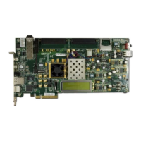
The KC705 board is populated with the Kintex-7 XC7K325T-2FFG900C FPGA.
For further information on Kintex-7 FPGAs, see
7 Series FPGAs Overview (DS180) [Ref 1].
FPGA Configuration
The KC705 board supports three of the five 7 series FPGA configuration modes:
• Master SPI flash memory using the onboard Quad SPI flash memory
• Master BPI flash memory using the onboard Linear BPI flash memory
• JTAG using a standard-A to micro-B USB cable for connecting the host PC to the KC705
board configuration port
Each configuration interface corresponds to one or more configuration modes and bus
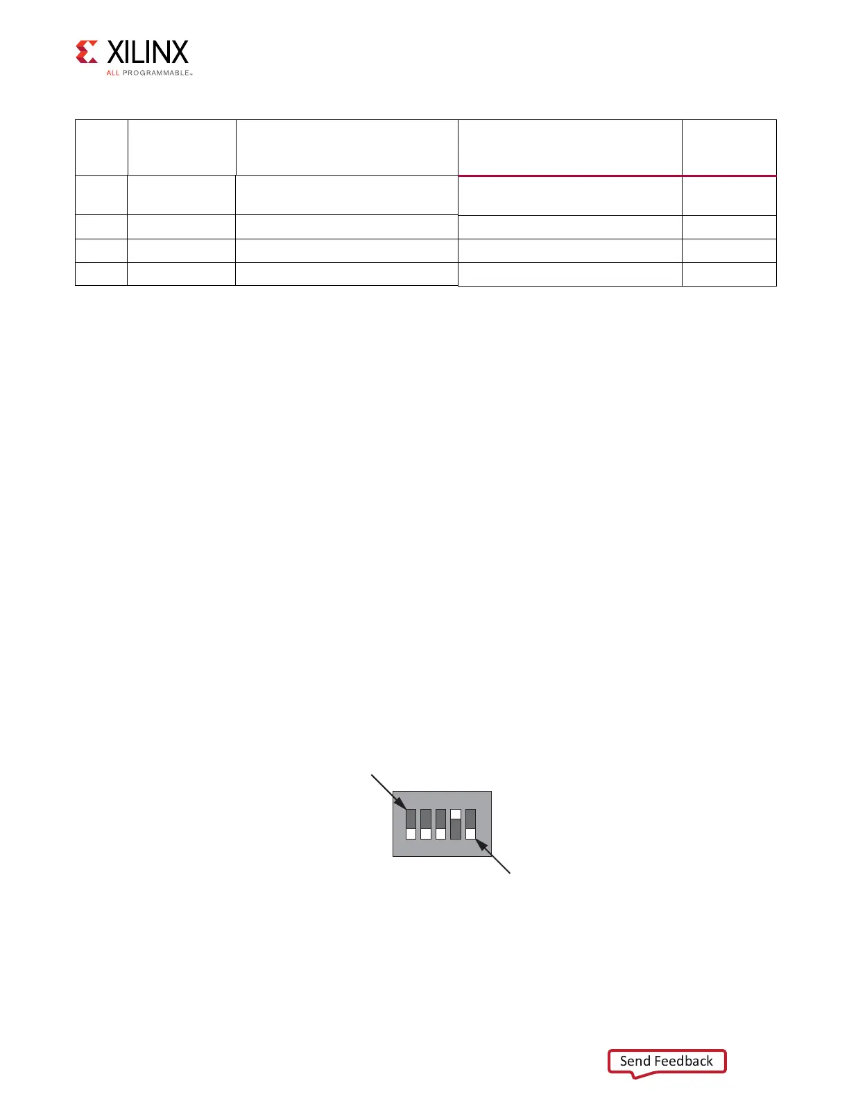
widths as listed in Table 1-2. The mode switches M2, M1, and M0 are on SW13 positions 3,
4, and 5 respectively as shown in Figure 1-3.
The default mode setting is M[2:0] = 010, which selects Master BPI at board power-on.
Refer to the Configuration Options, page 80 for detailed information about the mode
switch SW13.
34 J60 2 x 7 2 mm shrouded JTAG cable
connector
Molex 87832-1420 16
35 J39 2 x 5 shrouded PMBus connector Assman HW10G-0202 35
36 J49 12V power input 2 x 3 connector Molex 39-30-1060 35
37 SW7 CPU Reset Pushbutton E-Switch TL3301EP100QG 35
Table 1-1: KC705 Board Component Descriptions (Cont’d)
Callout
Reference
Designator
Component Description Notes
Schematic
0381397
Page Number
X-Ref Target - Figure 1-3
Figure 1-3: SW13 Default Settings
UG810_c1_03_011112
1
SW13
OFF Position = 0
ON Position = 1
2345
A25
A24
M2
M1
M0
 Loading...


