January 2007 115
Intel
®
855GME Chipset and Intel
®
6300ESB ICH Embedded Platform Design Guide
4.8.3.2 GMCH AGTL+ I/O Buffer Compensation
The HXRCOMP and HYRCOMP pins of the GMCH shall each be pulled-down to ground with a
27.4
Ω ± 1 percent resistor (see Figure 60). The maximum trace length from pin to resistor shall be
less than 0.5 inches and shall be 18 mil wide to achieve the Zo = 27.4
Ω target. Also, the routing
for HRCOMP shall be at least 25 mils away from any switching signal.
4.8.3.3 GMCH AGTL+ Reference Voltage
The GMCH's AGTL+ I/O buffer resistive compensation mechanism also requires the generation of
reference voltages to the HXSWING and HYSWING pins with a value of 1/3*VCCP.
Implementations for HXSWING and HYSWING voltage generation are illustrated in Figure 61.
Two resistive dividers with R1a = R1b = 301
Ω ± 1 percent and R2a = R2b = 150 Ω ±1 percent
generate the HXSWING and HYSWING voltages. C1a = C1b = 0.1 µF act as decoupling
capacitors and connect HXSWING and HYSWING to VCC_CORE. HSWING components shall
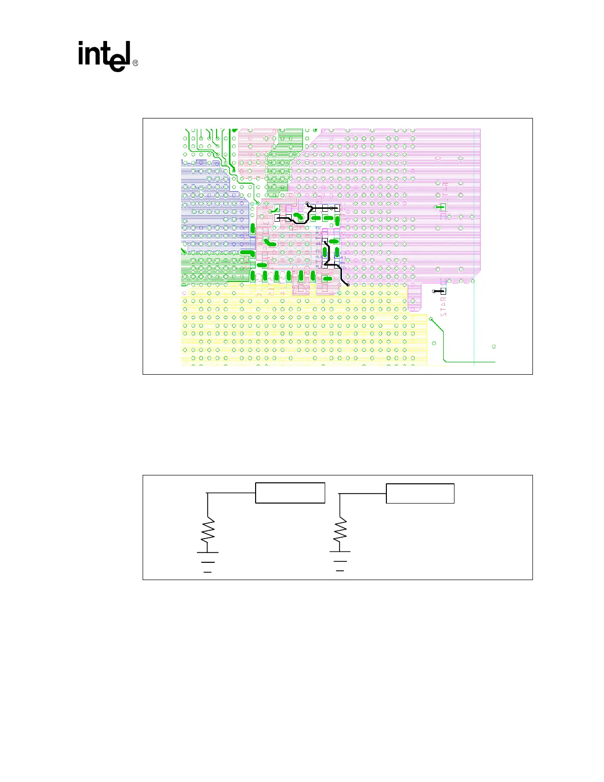
Figure 59. Secondary Side of the Motherboard Layout
Figure 60. GMCH HXRCOMP and HYRCOMP Resistive Compensation
27.4
Ω
±1%
HXRCOMP
27.4
Ω
±1%
HYRCOMP
 Loading...


