274
Intel
®
855GME Chipset and Intel
®
6300ESB ICH Embedded Platform Design Guide
Schematic Checklist Summary
12.3.1.2 DDR DIMM Interface Checklist
Table 122 presents the DDR DIMM interface checklist.
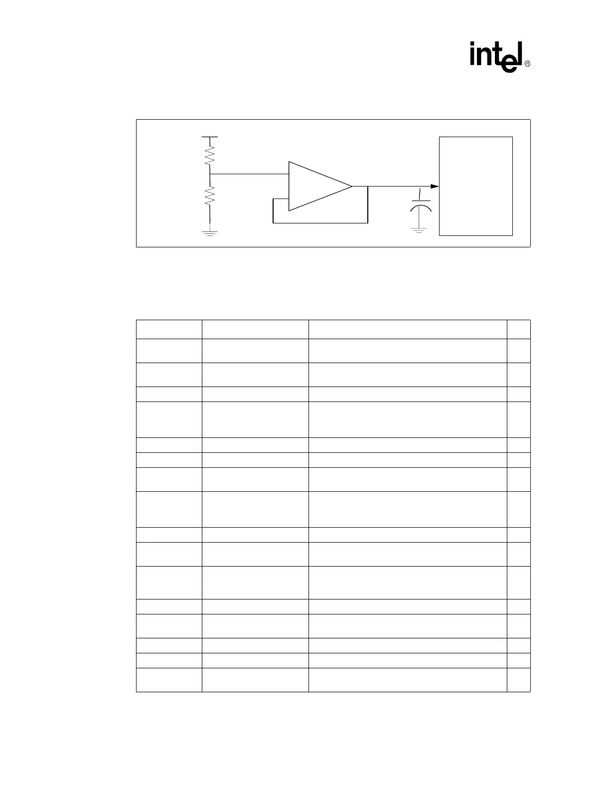
Figure 150. Reference Voltage Level for SMVREF
+
-
V_2P5_SM
0+/
-
1%
0+/
-
1 %
SMVREF
GMCH
SMVREF_0
0.1 uF
Table 122. DDR DIMM Interface Checklist
Pin Name Configuration Notes √
NC (FETEN)
(pin 167)
Signal may be left as NC (Not Connected).
CS[3:2]#
(pin163, 71)
Signal may be left as NC.
BA2 (pin 113) Signal may be left as NC.
VREF (pin 1)
Connected to 82855GME
SMVREF signal
Signal voltage level = V_2P5_SM/2.
Place a 0.1µF cap by GMCH, DIMM 0, and DIMM 1
pins.
VDD[9:1] Connect to V_2P5_SM Power must be provided during S3.
VDDSPD Connect to V_2P5_CORE
SA[2:1] Connect to GND
These lines are used for strapping the SPD address
for each DIMM.
SA0
DIMM 0: connect to GND
DIMM 1: connect to
V_2P5_SM
These lines are used for strapping the SPD address
for each DIMM.
VSS[22:1] Connect to GND
NC
(pin 10)
Signal may be left as NC.
SDA/SCL
Connect to the 6300ESB
SMBUS and SMLINK
through isolation circuitry.
NC (pin 90) Signal may be left as NC.
A13
(pin 103)
Signal may be left as NC.
VDDQ[16:1] Connect to V_2P5_SM
VDDID (pin 82) Signal may be left as NC.
NC[4:1] (pins
9,101,102,173)
Signal may be left as NC.
 Loading...


