January 2007 45
Intel
®
855GME Chipset and Intel
®
6300ESB ICH Embedded Platform Design Guide
Intel
®
Pentium
®
M/Celeron
®
M Processor FSB Design and Power Delivery Guidelines
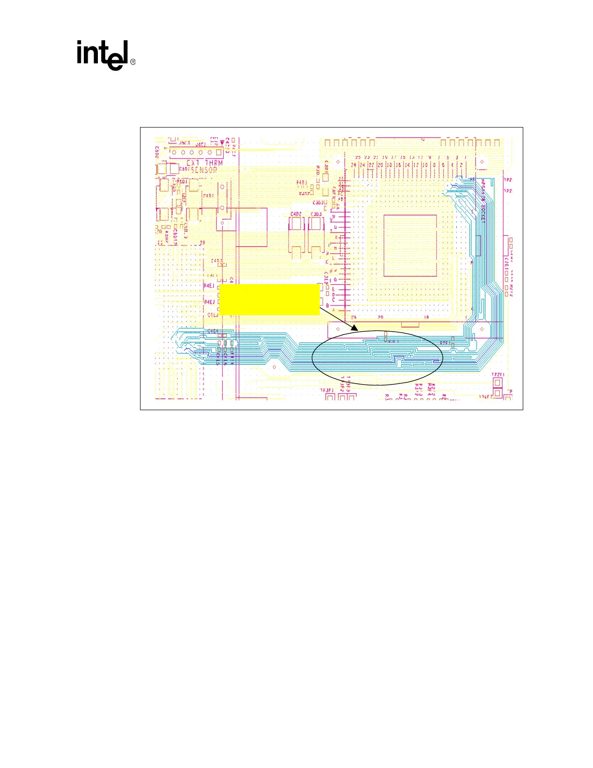
In a similar way, Figure 11 illustrates a recommended layout and stack-up example of how another
group of Intel Pentium M/Celeron M Processor FSB source synchronous DATA and ADDRESS
signals may reference ground planes on both Layer 2 and Layer 4. In the socket cavity of the Intel
Pentium M/Celeron M Processor, Layer 3 is used for VCC core power delivery to reduce the I*R
drop. However, outside of the socket cavity, Layer 3 signals are routed below a solid Layer 2
ground plane. Layer 4 is converted to a ground flood under the shadow of the Intel Pentium
M/Celeron M Processor FSB signals routing between the Pentium M/Celeron M processor and
GMCH. Figure 12 and Figure 13 depict example routing for Intel customer reference board.
Figure 10. Layer 6 Intel
®
Pentium
®
M/Celeron
®
M Processor System Bus
Source Synchronous Address Signals
Layer 6
FSB Address Signals
 Loading...


