146
Intel
®
855GME Chipset and Intel
®
6300ESB ICH Embedded Platform Design Guide
System Memory Design Guidelines (DDR-SDRAM)
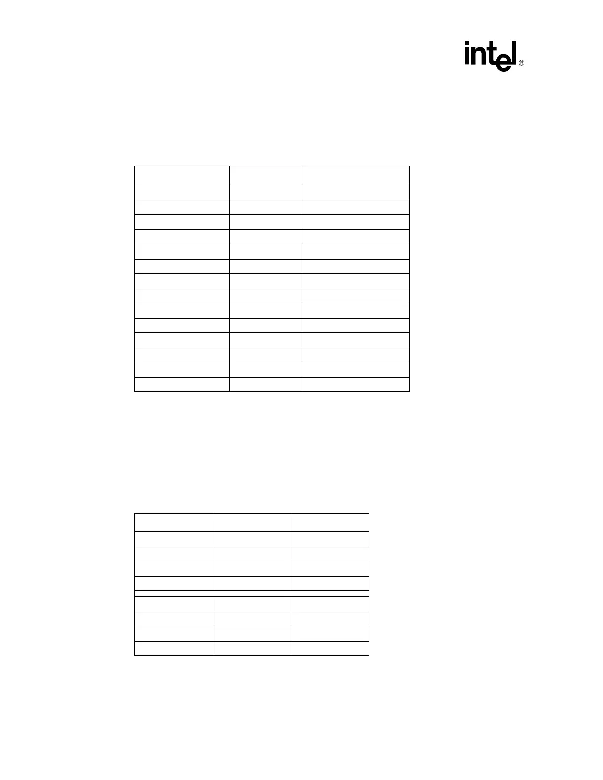
5.4.6.4 Command Group Package Length Table
The package length data in Table 39 shall be used to match the overall length of each command
signal to its associated clock reference length.
5.4.7 CPC Signals – SMA[5,4,2,1], SMAB[5,4,2,1]
The 82855GME control signals, SMA[5,4,2,1] and SMAB[5,4,2,1], are common clocked signals.
They are “clocked” into the DDR SDRAM devices using clock signals SCK[5:0]/SCK[5:0]#. The
GMCH drives the CPC and clock signals together, with the clocks crossing in the valid control
window. The GMCH provides one set of CPC signals per DIMM slot. Refer to Table 40 for the
SMA and SMAB signal to DIMM mapping.
Table 39. Command Group Package Lengths
Signal Pin Number Pkg Length (mils)
SMA[0] AC18 420
SMA[3] AD17 472
SMA[6] AD8 591
SMA[7] AD7 596
SMA[8] AC6 630
SMA[9] AC5 681
SMA[10] AC19 377
SMA[11] AD5 683
SMA[12] AB5 609
SBA[0] AD22 592
SBA[1] AD20 435
SCAS# AC24 562
SRAS# AC21 499
SWE# AD25 751
Table 40. Control Signal to DIMM Mapping
Signal Relative To DIMM Pin
SMA[1] DIMM0 AD14
SMA[2] DIMM0 AD13
SMA[4] DIMM0 AD11
SMA[5] DIMM0 AC13
SMAB[1] DIMM1 AD16
SMAB[2] DIMM1 AC12
SMAB[4] DIMM1 AF11
SMAB[5] DIMM1 AD10
 Loading...


