226
Intel
®
855GME Chipset and Intel
®
6300ESB ICH Embedded Platform Design Guide
Intel
®
6300ESB Design Guidelines
Table 91. PCI Data Signals Routing Summary
Trace
Impedance
PCI Routing Requirements Topology
Maximum Trace Length
L1 L2 L3 L4
55
Ω ± 10%
5 mils width, 7 mils spacing
(based on stackup
assumptions in Section 3.1)
2 Slots
W1 = W2 = 0.5 inches,
R_IDSEL = 300 to 900
Ω
10
inches
1.0
inch
3 Slots
W1 = W2 = 0.5 inches,
R_IDSEL = 300 to 900 Ω
10
inches
1.0
inch
1.0
inch
4 Slots
W1 = W2 = 0.5 inches,
R_IDSEL = 300 to 900
Ω
10
inches
1.0
inch
1.0
inch
1.0
inch
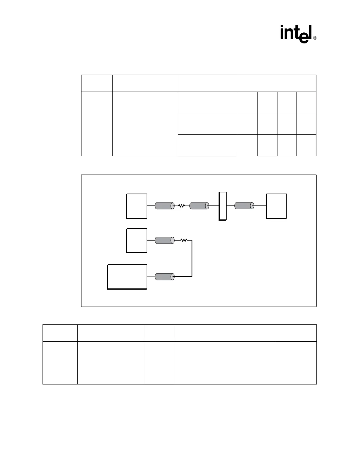
Figure 120. PCI 33MHz Clock Layout Example
Table 92. PCI 33 MHz Clock Signals Routing Summary
Trace
Impedance
PCI Routing Requirements Topology Maximum Trace Length Resistor Values
55
Ω ± 10%
5 mils width, 50mils spacing
(based on stackup
assumptions in Section 3.1)
2 -4
Devices
W1 = 0.5 inches
W2 = W5 – 4.5”
W3 = 2.5 inches (Shown as a reference only)
W4 = 0.5 inches
W5 = May be as long as needed as long as
W2 is scaled accordingly
R1 = 33
Ω
R2 = 33 Ω
B1172-02
W5
W2W1
R1
CK409
PCI
W4
R2
CK409
Note: Clocks should be routed first.
W3
Connector
Intel
®
6300ESB
I/O Controller
Hub
 Loading...


