January 2007 277
Intel
®
855GME Chipset and Intel
®
6300ESB ICH Embedded Platform Design Guide
Schematic Checklist Summary
12.3.3 Hub Interface Checklist
Table 125 presents the hub interface checklist.
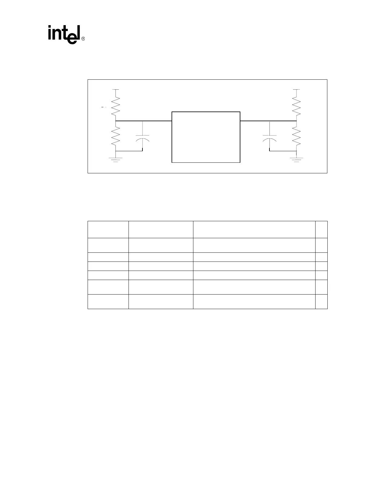
Figure 151. Intel
®
855GME Chipset HXSWING and HYSWING Reference
Voltage Generation Circuit
01
50
C1a
+VCCP
GMCH
HXSWING
HXSWING
HYSWING
301
1%
150
1%
C1b
+VCCP
HYSWING]
Table 125. Hub Interface Checklist
Pin Name
System
Pull-up/Pull-down
Notes √
Hl[10:0]
Connect to the 6300ESB (HI[10:0] signals). Refer to
Section 8.1 for more information.
HLSTB (S) Connect to the 6300ESB (HL_STBS signal).
HLSTB# (F) Connect to the 6300ESB (HL_STBF signal).
HLVREF Refer to Section 8.1.4.2. Signal voltage level = 0.35 V ± 8%.
PSWING Refer to Section 8.1.4.2.
Signal voltage level = 2/3 of V1P2_GMCH or
0.8 V ± 8%.
HLRCOMP
37.4
Ω 1% pull-up to 1.35V
core voltage
Refer to Section 8.1.5 for more information.
 Loading...


