262
Intel
®
855GME Chipset and Intel
®
6300ESB ICH Embedded Platform Design Guide
Platform Clock Routing Guidelines
Motherboard Impedance – Differential 100 Ω typical 4
Routing Length –
L1, L1’: Clock Driver to Rs
0.5 inch max Figure 146 6, 7
Routing Length –
L2, L2’: Rs to Rs-Rt Node
0 – 0.2 inch Figure 146 6, 7
Routing Length –
L3, L3’: Rs-Rt Node to Rt
0 – 0.2 inch Figure 146 6, 7
Routing Length –
L4, L4’: Rs-Rt Node to Load
2 – 15 inches Figure 146
SCR – SCR# Length Matching ± 10 mils
Rs Series Termination Value 33
Ω ± 5% Figure 146
Rt Shunt Termination Value
49.9
Ω± 5%
(for 55
Ω odd mode MB
impedance)
Figure 146 5
NOTES:
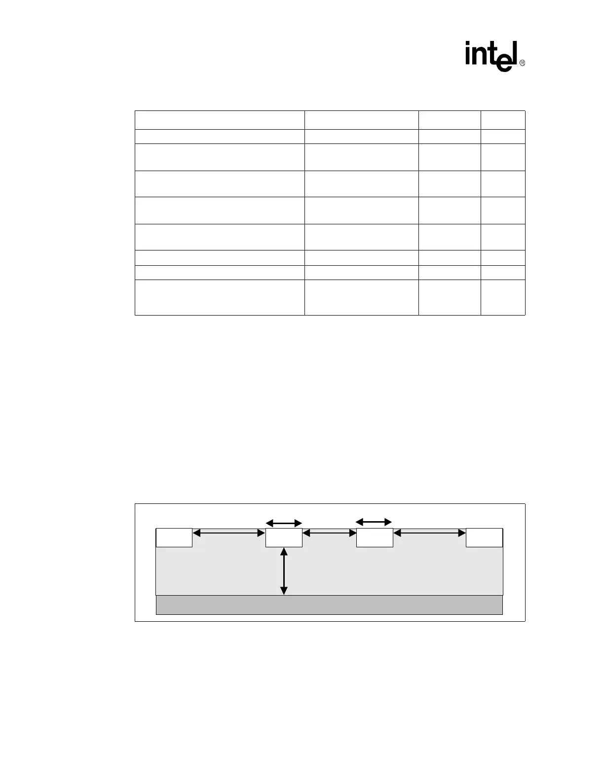
1. Edge to edge spacing between the two traces of any differential pair. Uniform spacing should be
maintained along the entire length of the trace.
2. Clock traces are routed in a differential configuration. Maintain the minimum recommended spacing
between the two traces of the pair. Do not exceed the maximum trace spacing, as this will degrade the
noise rejection of the network
3. Set line width to meet correct motherboard impedance. The line width value provided here is a
recommendation to meet the proper trace impedance based on the recommended stack up.
4. The differential impedance of each clock pair is approximately 2*Zsingle-ended*(1-2*Kb) where Kb is the
backwards cross-talk coefficient. For the recommended trace spacing, Kb is very small, and the effective
differential impedance is approximately equal to 2 times the single-ended impedance of each half of the
pair.
5. Rt shunt termination value should match the motherboard impedance.
6. Minimize L1, L2 and L3 lengths. Long lengths on L2 and L3 degrade effectiveness of source termination
and contribute to ringback.
7. The goal of constraining all bus clocks to one physical routing layer is to minimize the impact on skew due
to variations in Er and the impedance variations due to physical tolerances of circuit board material.
Figure 147. Trace Spacing for SRC Clocks
Table 114. SCR/SCR# Routing Guidelines (Sheet 2 of 2)
Layout Guideline Value Illustration Notes
h
S
WW
S1
S1
SRC SRC#
Ground Plane
 Loading...


