270
Intel
®
855GME Chipset and Intel
®
6300ESB ICH Embedded Platform Design Guide
Schematic Checklist Summary
12.2 CK409 Clock Checklist
12.2.1 Connection Recommendations
Table 120 presents the CK409 connection recommendations.
#3
Low Frequency Decoupling (Polymer
Covered Aluminum – SP Cap, A0
Cap)
5 x 330 µF 15 mΩ (max)/5 3.5 nH/5
Low Frequency Decoupling
(1206 MLCC, >= X5R)
25 x 10 µF 5 m
Ω (typ)/25 1.2 nH/25
Mid Frequency Decoupling
(0612 MLCC, >= X5R)
15 x 2.2 µF 5 m
Ω (typ)/15 0.2 nH/15
#4
(Note 1)
Low-Frequency Decoupling (Polymer
Covered Aluminum – SP CAP, AO
Cap)
4 x 220
μF12mΩ (max)/4 3.5 nH/4
Mid-Frequency Decoupling
(0805 MLCC>= X5R)
35 x 10
μF5mΩ (typ)/35 0.6 nH/35
Table 119. VCC (CORE) Decoupling Recommendations (Sheet 2 of 2)
Option Description C, μF ESR, mΩ ESL, nH √
NOTES:
1. Decoupling guidelines are recommendations based on Intel reference board design. The Intel Customer
Reference Board uses option #4. This is the preferred recommendation for decoupling.
2. When deciding on overall decoupling solution, customers may need to take layout and PCB board design
into consideration.
3. Option #4 is to be used with small footprint (100 mm
2
or less) 0.36 µH ± 20% inductors.
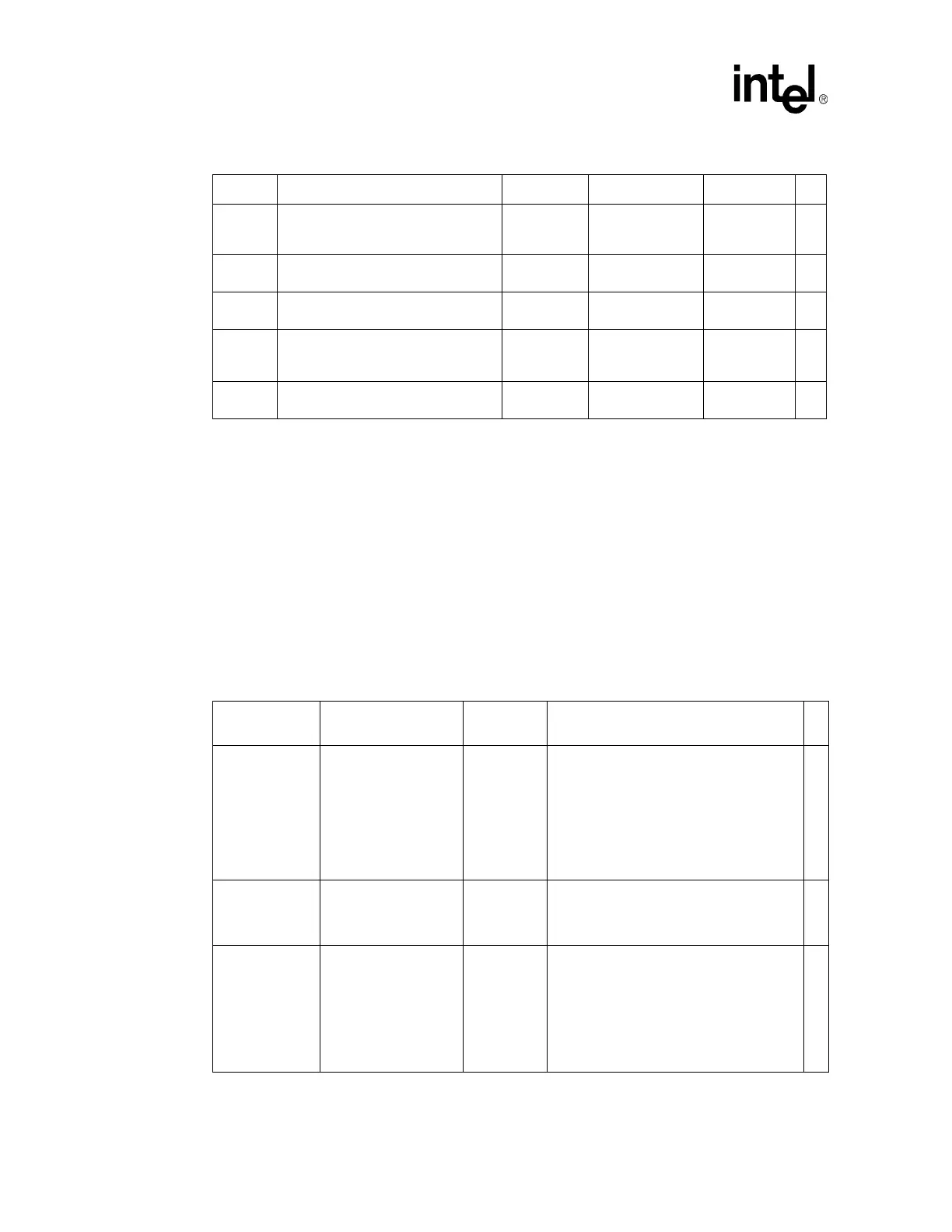
Table 120. CK409 Connection Recommendations (Sheet 1 of 2)
Pin Name
System
Pull-up/Pull-down
Series
Resistor
Notes
√
3V66_[0]
3V66_[1]*
33
Ω ±5%
When the signal is used, one 33 ohm series
resistor is required. When the signal is NOT
used, it shall be left as NC (Not Connected)
or connected to a test point.
*Two possible topologies for 3V66_1:
• Use directly for GMCH’s DREFSSCLK.
• Use as input to an SSC device with SSC
output to GMCH’s DREFSSCLK.
3V66_[4:2] 33
Ω ±5%
The Intel CRB routes 3V66[2] (pin 21) to
GCLKIN on GMCH. The other two signals
route to 6300ESB (CLK66) and AGP
connector (AGPCLK).
CPU[0], CPU[0]#
CPU[1], CPU[1]#
CPU[2], CPU[2]#
49.9
Ω ± 1%
pull- down to GND
33
Ω ±5%
Use one pair for the
processor and another
pair for GMCH. When onboard ITP is
implemented, the third pair of clock signals
is used for the ITP connector. Otherwise, it
may be routed to the dedicated ITP clock
pins on the processor socket.
Refer to Chapter 11 for all routing
requirements.