January 2007 271
Intel
®
855GME Chipset and Intel
®
6300ESB ICH Embedded Platform Design Guide
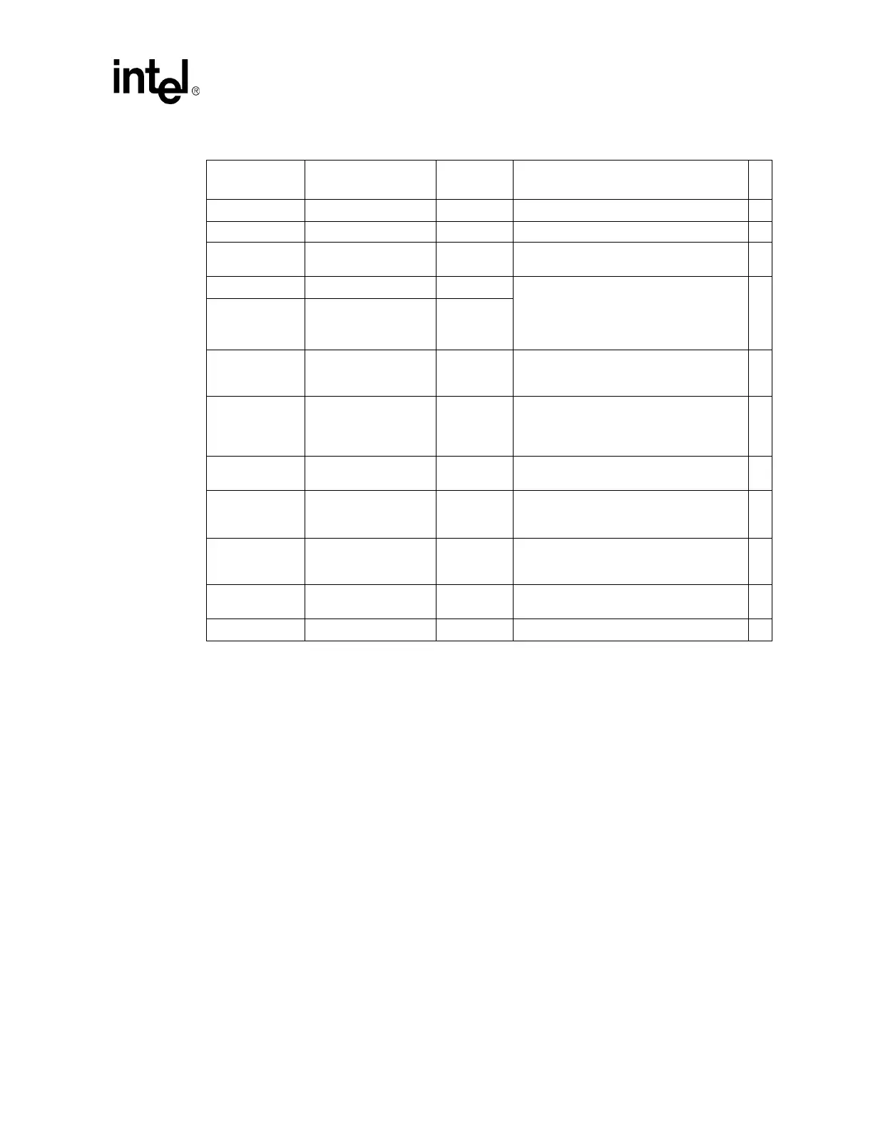
Schematic Checklist Summary
DOT_48MHZ 33 Ω ± 5% Connect to GMCH’s DREFCLK.
FS_A, FS_B Used for selecting the host clock frequency.
IREF
475
Ω ± 1%
pull-down to GND
Adjusts IREF to 2.32 mA.
PCI[6:0] 33
Ω ± 5% Connect to various PCI devices and other
33 MHZ clock inputs for devices such as
FWH and SIO (LPC). Use one clock for the
6300ESB. Unused clock pins shall be left as
NC or connected to a test point.
PCIF[2:0] 33
Ω ±5%
PWRDWN#
Terminate to
VCC3_CLK through
1K
Ω resistor.
The Intel CRB does not support S1M state.
REF[0:1] 33
Ω ±5%
This is the 14.318 MHz clock reference
signal for the 6300ESB, SIO and LPC. Each
receiver requires one 33-ohm series
resistor.
USB_48MHZ 33
Ω ±5%
Connect to the 6300ESB’s 48 MHz clock
input.
XTAL_IN,
XTAL_OUT
Terminate each pin to
GND through a
10 pF ± 5% capacitor.
Connect to a 14.318 MHz crystal, placed
within 500 mils of CK409.
VDD[7:0],
VDDA,
VDD_48MHZ
Connect to VCC3.
Refer to clock vendor datasheet for
decoupling info.
VSS[5:0], VSSA,
VSS_48MHZ
Connect to GND.
VSSIREF Connect to GND.
Table 120. CK409 Connection Recommendations (Sheet 2 of 2)
Pin Name
System
Pull-up/Pull-down
Series
Resistor
Notes
√
 Loading...


