January 2007 63
Intel
®
855GME Chipset and Intel
®
6300ESB ICH Embedded Platform Design Guide
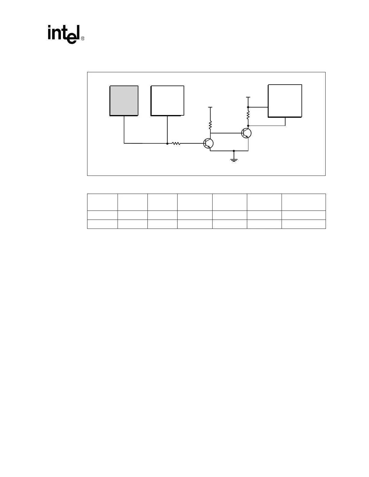
4.1.5.7 Voltage Translation Logic
A voltage translation circuit or component is required on any signals where the voltage signaling
level between two components connected by a transmission line may cause unpredictable signal
quality. The recommended voltage translation circuit for the platform is shown in Figure 22. For
the INIT# signal (Section 4.1.5.6), a specialized version of this voltage translator circuit is used
where the driver isolation resistor, Rs, is place at the beginning of a transmission line that connects
to the first bipolar junction transistor, Q1. Though the circuit shown in Figure 22 was developed to
work with signals that require translation from a 1.05 V to a 3.3 V voltage level, the same topology
and component values, in general, may be adapted for use with other signals as well, provided the
interface voltage of the receiver is also 3.3 V. Any component value changes or component
placement requirements for other signals must be simulated in order to ensure good signal quality
and acceptable performance from the circuit.
In addition to providing voltage translation between driver and receiver devices, the recommended
circuit also provides filtering for noise and electrical glitches. A larger first-stage collector resistor,
R1, may be used on the collector of Q1, however, it results in a slower response time to the output
falling edge. In the case of the INIT# signal, resistors with values as close as possible to those listed
in Figure 22 shall be used without exception.
With the low 1.05 V signaling level of the Intel Pentium M/Celeron M processor system bus, the
voltage translation circuit provides ample isolation of any transients or signal reflections at the
input of transistor Q1 from reaching the output of transistor Q2. Based on simulation results, the
voltage translation circuit may effectively isolate transients as large as 200 mV and that last as long
as 60 ns.
Figure 21. Routing Illustration for Topology 3
Table 16. Layout Recommendations for Topology 3
L1 + L2 L3 L4 Rs R1 R2
Transmission
Line Type
0.5” – 12.0” 0” – 3.0” 0.5” – 6.0” 330 Ω ±5% 1.3kΩ ±5% 330Ω ± 5% Micro-strip
0.5” – 12.0” 0” – 3.0” 0.5” – 6.0” 330
Ω ±5% 1.3kΩ ± 5% 330 Ω ± 5% Strip-line
B3161-01
FWH
V_IO_FWH
R2
R1
Rs
3904
L4
L1L2
L3
3.3V
3.3V
Q2
Q1
3904
CPU
Intel
®
6300ESB
I/O
Controller
 Loading...


