Design Guide 177
Intel
®
855GME Chipset and Intel
®
82801DB ICH4 Embedded Platform Design Guide
AGP Port Design Guidelines
7.2.2.3 Trace Length Mismatch Requirements
The trace length minimum and maximum (relative to strobe length) should be applied to each set of
2X/4X timing domain signals independently. If AD_STB0 is 5 inches and ADSTB0# is 5.01
inches, then AD[15:0] and C/BE[1:0] must be between 4.91 inches and 5.1 inches. However,
AD_STB1 and ADSTB1# can be 3.5 inches and 3.51 inches (and therefore AD[31:16] and C/
BE#[3:2] must be between 3.41 inches and 3.6 inches). In addition, all 2X/4X timing domain
signals must meet the maximum trace length requirements.
• All signals should be routed as strip lines (inner layers).
• All signals in a signal group should be routed on the same layer. Routing studies have shown
that these guidelines can be met. The trace length and trace spacing requirements must not be
violated by any signal. Trace length mismatch for all signals within a signal group should be as
close to 0 inches as possible to provide optimal timing margin.
The strobe pair must be length matched to less than ± 0.01 inches (that is, a strobe and its
compliment must be the same length within ± 0.01 inches).
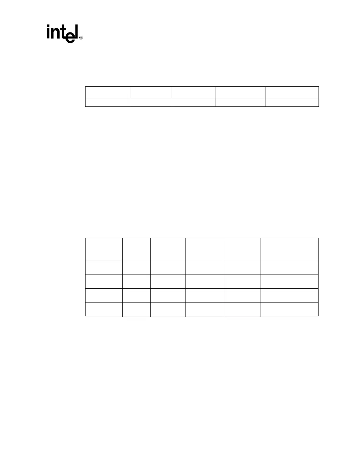
Table 62 shows the AGP 2.0 routing summary.
7.2.3 AGP Clock Skew
The maximum total AGP clock skew between the GMCH and the graphics component is 1 ns for
all data transfer modes. This 1 ns includes skew and jitter, which originates on the motherboard,
add-in module (if used), and clock synthesizer. Clock skew must be evaluated not only at a single
threshold voltage, but also at all points on the clock edge that falls in the switching range. The 1 ns
skew budget is divided such that the motherboard is allotted 0.9 ns of clock skew (the motherboard
designer shall determine how the 0.9 ns is allocated between the board and the synthesizer).
Table 61. AGP 2.0 Data Lengths Relative to Strobe Length
Max Trace Length Trace Spacing Strobe Length Min Trace Length Max Trace Length
< 6 in 1:2 X X - 0.1 in X + 0.1 in
Table 62. AGP 2.0 Routing Guideline Summary
Signal
Maximum
Length
Trace
Spacing (4
mil traces)
Length
Mismatch
Relative To Notes
1X Timing
Domain
10 in 4 mils No Requirement N/A None
2X/4X Timing
Domain Set#1
6 in 8 mils ± 0.1 in
AD_STB0 and
AD_STB0#
AD_STB0, AD_STB0#
must be the same length
2X/4X Timing
Domain Set#2
6 in 8 mils ± 0.1 in
AD_STB1 and
AD_STB1#
AD_STB1, AD_STB1#
must be the same length
2X/4X Timing
Domain Set#3
6 in 8 mils ± 0.1 in
SB_STB and
SB_STB#
SB_STB, SB_STB#
must be the same length
 Loading...


