184
Intel
®
855GME Chipset and Intel
®
6300ESB ICH Embedded Platform Design Guide
Hub Interface
8.1.2 8-Bit Hub Interface Signal Referencing
The 8-bit Hub Interface data signal traces (HI[11:0]) and the two Hub Interface strobe signals
(HI_STB/HI_STBS and HI_STB#/HI_STBF) must all be referenced to ground to insure proper
noise immunity.
8.1.3 8-Bit Hub Interface Strobe Signals
The Hub Interface strobe signals should be routed 5 mil width, 15 mil spacing. (See Table 67.) This
strobe pair should have a minimum of 20 mils spacing from any adjacent signals.
8.1.4 8-bit Hub Interface HIREF and HI_VSWING Generation/
Distribution
HIREF is the Hub Interface reference voltage. The 6300ESB uses HI_VSWING to control voltage
swing and impedance strength of the Hub Interface buffers. The HIREF and HI_VSWING voltage
requirement and associated resistor recommendations for the voltage divider circuit are listed in
Table 68. Four options are given for the divider circuit, choose the one that best supports your
platform.
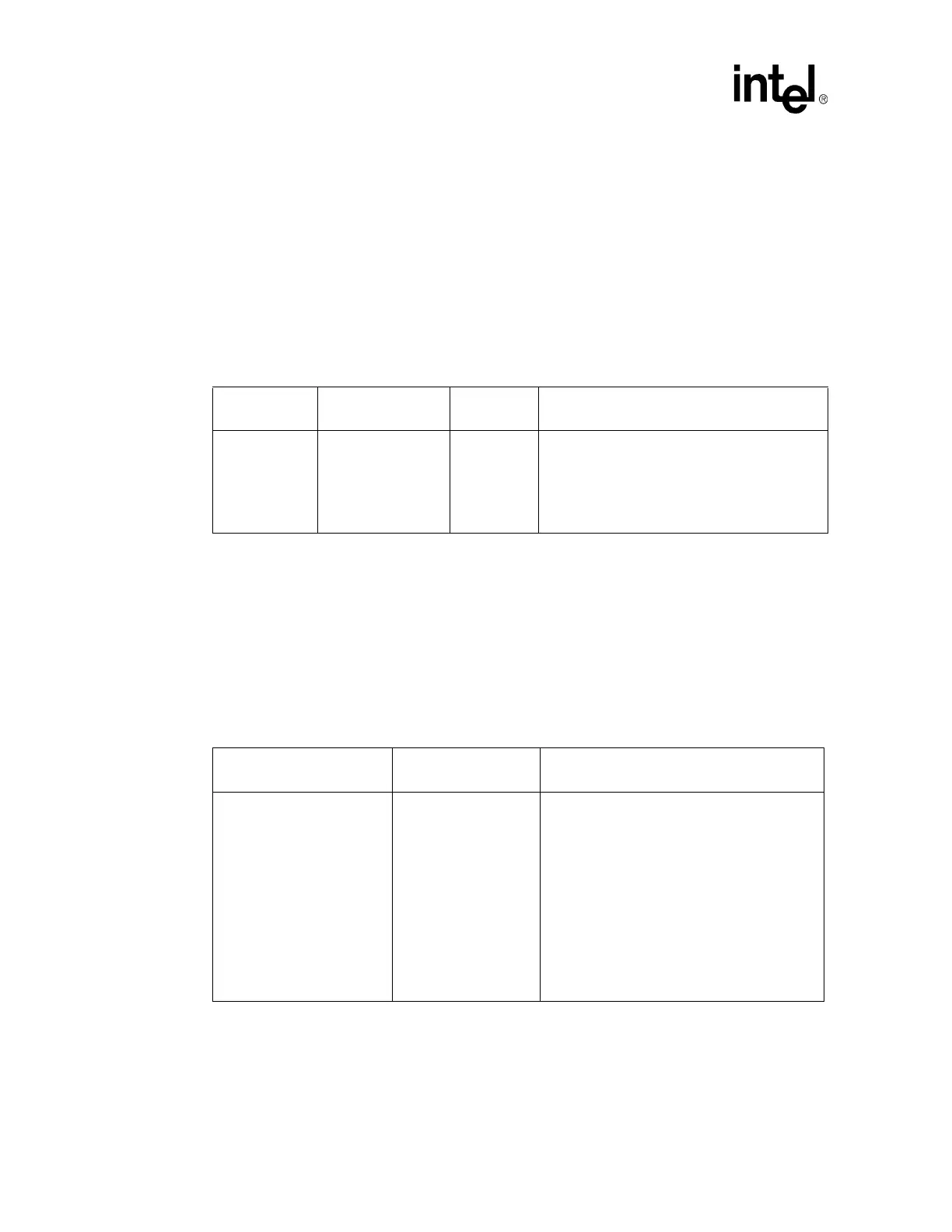
Table 67. Hub Interface 1.5 Strobe Signals Routing Summary
Strobe Signal
Requirements
Maximum Trace
Length
Referencing Strobe Signal Length Matching
5 mil width,
20 mil spacing
(from other
signals),
15 mil spacing
(intra-pair)
8 inches Ground
Each strobe signal must be the same length, and
each data signal must be matched within ± 0.25
inches of the strobe signal.
Table 68. 8-Bit Hub Interface HIREF/HI_VSWING Generation Circuit Specifications
HIREF Voltage
Specification (V)
HI_VSWING Voltage
Specification (V)
Recommended Values for the HIREF/
HI_VSWING Divider Circuit (
Ω)
350 mV
± 2% 800 mV ± 2%
Option A (Figure 86& Figure 87)
R1 = 226
Ω ± 1%, R2 = 147 Ω ± 1%,
R3 = 113
Ω ± 1%
Option B (Figure 86& Figure 87)
R1 = 80.6
Ω ± 1%, R2 = 51.1 Ω ± 1%,
R3 = 40.2
Ω ± 1%
Option C (Figure 86& Figure 87)
R1 = 255
Ω ± 1%, R2 = 162 Ω ± 1%,
R3 = 127
Ω ± 1%
Option D (Figure 88& Figure 89)
R4 = 78.7
Ω ± 1%, R5 = 24.2 Ω ± 1%,
R6 = 43.2
Ω ± 1%, R7 = 49.9 Ω ± 1%
NOTES:Capacitance Values For All Options
7. C1 and C3 = 0.1 µF (near divider)
8. C2, C4, C5, C6 = 0.01 µF (near GMCHGMCH and 6300ESB)
9. The resistor values R1, R2, R3, R4, R5, R6, and R7 must be rated at 1% tolerance.