January 2007 167
Intel
®
855GME Chipset and Intel
®
6300ESB ICH Embedded Platform Design Guide
Integrated Graphics Display Port
6.3.3 DVOB and DVOC Assumptions, Definitions, and
Specifications
The source synchronous solution space consists of all designs in which the flight time mismatch
between a strobe and its associated data is less than the total allowable skew:
T
skew
= T
flightdata
- T
flightstrobe
Where T
flightdata
and T
flightstrobe
are the driver-pad-to-receiver-pin flight times of the data and the
strobe respectively.
The DVO physical interface is a point-to-point topology using 1.5 V signaling. The DVO uses a
165 MHz clock.
The flight time skew simulations reproduce all parameters that could cause a skew between two
signals, including motherboard and add-in card line lengths, effective capacitance in the buffer
models, crosstalk on each of the different interconnect combinations, data pattern dependencies,
and ISI induced skews.
6.3.4 DVOB and DVOC Simulation Method
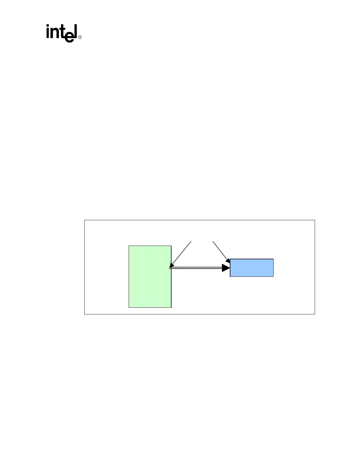
A model for simulation purposes is shown in Figure 78. The DVO component is a third party-chip.
Figure 78. DVOB and DVOC Simulations Model
GMCH
DVO I/F
(Device)
DVOB/DVOC
Control, Data
tDVb, tDVa
tDSu, tDh
 Loading...


