January 2007 121
Intel
®
855GME Chipset and Intel
®
6300ESB ICH Embedded Platform Design Guide
4.8.10 6300ESB Power Signal Decoupling
4.8.11 Hub Interface Decoupling
Refer to Section 8.1.6 for details.
4.8.12 FWH Decoupling
A 0.1 µF capacitor shall be placed between the VCC supply pins and the VSS ground pins to
decouple high-frequency noise, which may affect the programmability of the device. Additionally,
a 4.7
µF capacitor should be placed between the V
CC
supply pins and the V
SS
ground pins to
decouple low frequency noise. The capacitors should be placed no further than 390 mils from the
V
CC
supply pins. Note that the value of the low-frequency bulk decoupling capacitor is dependent
on board layout and system power supply design.
4.9 Thermal Design Power
Refer to the Intel
®
855GME Chipset Memory Controller Hub (MCH) Thermal Design Guide for
Embedded Applications and the Intel
®
6300ESB I/O Controller Hub Thermal and Mechanical
Design Guide for information on thermal design.
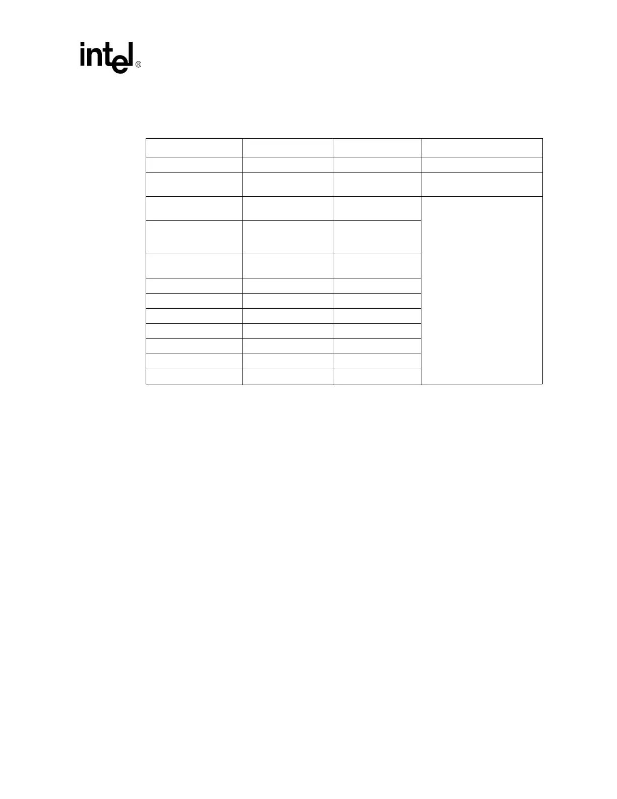
Table 26. Power Signal Decoupling
Pin Capacitor Quantity Decoupling Placement
V_CPU_IO 0.1 µF 1 Close to the 6300ESB
V
CC
RTC 0.1 µF 2
One close to the 6300ESB and
one close to the battery
V
CC
3.3
0.1 µF
0.01µF
12
4
Close to the 6300ESB
V
CC
Sus3.3
0.1 µF
0.01 µF
1.0 µF
4
1
1
V
CC
1_5
0.1 µF
0.01 µF
6
2
V
CC
Sus1_5 0.1 µF 4
V5REF_Sus 0.1 µF 1
V5REF 0.1 µF 1
V
CC
PLL 0.1 µF 3
V
CC
HI 0.1 µF 2
VCCREF (3.3 V) 1.0 µF 1
VCCA 0.1 µF 1
 Loading...


