January 2007 279
Intel
®
855GME Chipset and Intel
®
6300ESB ICH Embedded Platform Design Guide
Schematic Checklist Summary
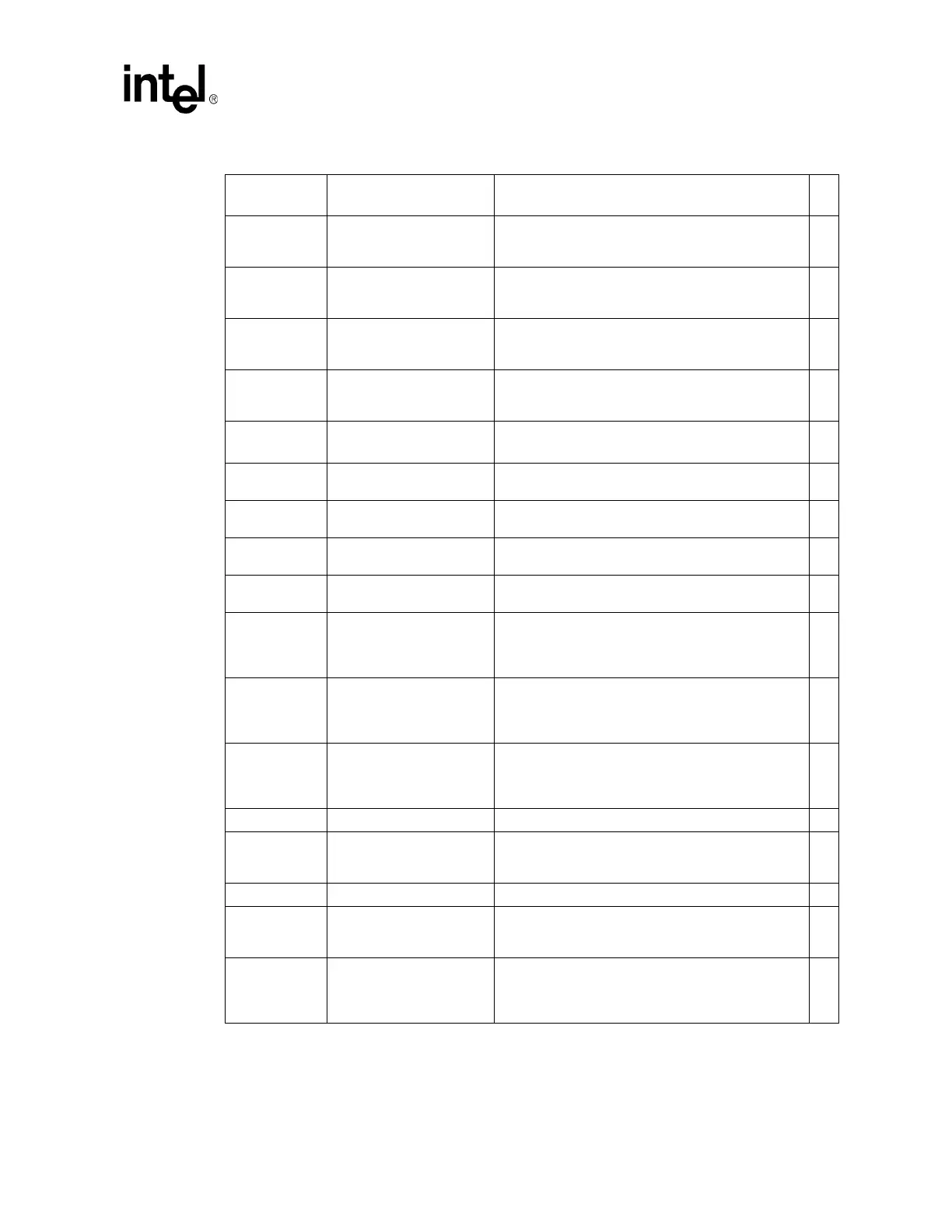
DVOCFLDSTL 100 KΩ pull-down to GND
Pull-down resistor required only if signal is unused
(10 K-100 K). It is up to DVO device to drive this signal.
For AGP this signal is: GAD[31].
DVOBCINTR#
100 K
Ω pull-up to
V_1P5_CORE
Pull-up resistor required only if signal is unused
(10 K-100 K). It is up to the DVO device to drive this
signal. For AGP this signal is: GAD[30].
DVOBCCLKINT 100 K
Ω pull-down to GND
Pull-down resistor required only if signal is unused
(10 K-100 K). It is up to the DVO device to drive this
signal. For AGP this signal is: GAD[13].
DVOBD[11:0]
When this port is unused, it may be left as NC. For
AGP these signals are: GAD[12:2]. Refer to Chapter
3.6.3 of the 855GME datasheet for exact assignment.
DVOBCLK,
DVOBCLK#
When this port is unused, it may be left as NC.
For AGP these signals are: AD_STB0, AD_STB0#
DVOBHSYNC
When this port is unused, it may be left as NC. For
AGP this signal is: GAD[0].
DVOBVSYNC
When this port is unused, it may be left as NC. For
AGP this signal is: GAD[1].
DVOBBLANK#
When this port is unused, it may be left as NC. For
AGP this signal is: GCBE#1.
DVOBFLDSTL
(pin M2)
100 K
Ω pull-down to GND
Pull-down resistor required only if this signal is unused
(10K-100K). For AGP this signal is: GAD[14].
MI2CCLK,
MI2CDATA
2.2 K
Ω pull-up to
V_1P5_CORE
Pull-up resistor required on each signal even if they are
unused (2.2 K-100 K). This signal is 1.5 V tolerant. It
may require voltage translation circuit. For AGP these
signals are: GIRDY#, GDEVSEL#.
MDVICLK,
MDVIDATA
2.2 K
Ω pull-up to
V_1P5_CORE
Pull-up resistor required on each signal even if they are
unused (2.2 K-100 K). This signal is 1.5 V tolerant. It
may require voltage translation circuit. For AGP these
signals are: GTRDY#, GFRAME#.
MDDCCLK,
MDDCDATA
2.2 K
Ω pull-up to
V_1P5_CORE
Pull-up resistor required on each signal even if they are
unused (2.2 K-100 K). This signal is 1.5 V tolerant. It
may require voltage translation circuit. For AGP these
signals are: GSTOP#, GAD[15].
ADDID[6:0] Leave as NC. For AGP these signals are: GSBA[6:0].
ADDID7
1K
Ω pull-down to GND if
DVO device is onboard
When DVO interface is not used, this signal may be left
as NC. Otherwise, pull-down is needed. For AGP this
signal is: GSBA[7].
GCLKIN 33 ohm series at CK409 Connect to CK409, 66 MHz clock.
DVODETECT
1K
Ω pull-up to
V_1P5_CORE if DVO
interface is unused
When DVO interface is used, leave as NC. This signal
has internal pull-down. For AGP this signal is: GPAR.
DPMS
Connect to 1.5 V version of the 6300ESB’s SUSCLK or
a clock that runs during S1. For AGP this signal is:
GPIPE. See Section 7.2.11 for the DPMS clock
isolation circuit.
Table 127. DVO Checklist (Sheet 2 of 2)
Pin Name System
Pull-up/Pull-down
Notes
√
 Loading...


