Revision:1.0(2023-01-12)
46
22..33..44..22 Frontend of the Main Board
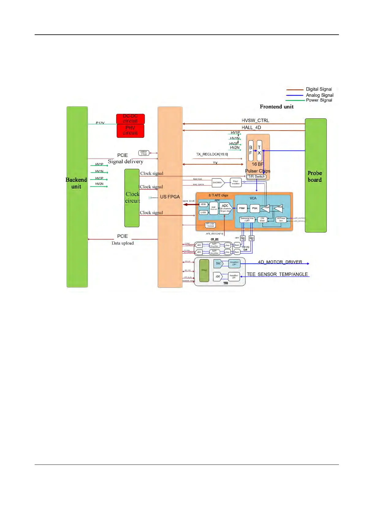
Figure2–5 Block diagram of the main board front end
The block diagram of the main board front end is shown in the preceding figure. The transmission
and reception solution consists of eight MAX chips and eight AFE chips. The transmission and
reception control and signal processing are all realized through the FE FPGA. The major
functions of the main board front end are as follows:
1. Transmission: The front-end FPGA controls 128 channels to transmit high-voltage ultrasonic
signals to the probe, so as to realize transmission focusing of the machine.
2. Reception: The front-end FPGA controls 128 channels to receive ultrasonic echo signals from
the probe, so as to realize reception focusing of the machine.
3. The ATGC module implements automatic gain compensation so that the brightness of the
ultrasound image in the far and near fields is consistent.
4. Support for data caching through the IQ (frame buffer), UP (upload), SCAN (scan), AD
(analogue-to-digital conversion) channels.
5. Generation and delivery of front-end clock signals.
6. Imaging-related logic functions, which are carried by the front-end FPGA.
• Scan controller
• Parsing of imaging parameters transmitted by the back end
Diagnostic Ultrasound System
Service Manual
2 Product Knowledge
 Loading...