Home
Renesas
Computer Hardware
RL78 Series
Renesas RL78 Series User Manual
4
of 1
of 1 rating
1879 pages
Give review
Manual
Specs
To Next Page
To Next Page
To Previous Page
To Previous Page
Loading...
RL78/F13, F14
CHAPTER 18 CAN INTERF
ACE (RS-CAN LITE)
R01UH0368EJ021
0 Rev
.2.10
1407
Dec 10, 2015
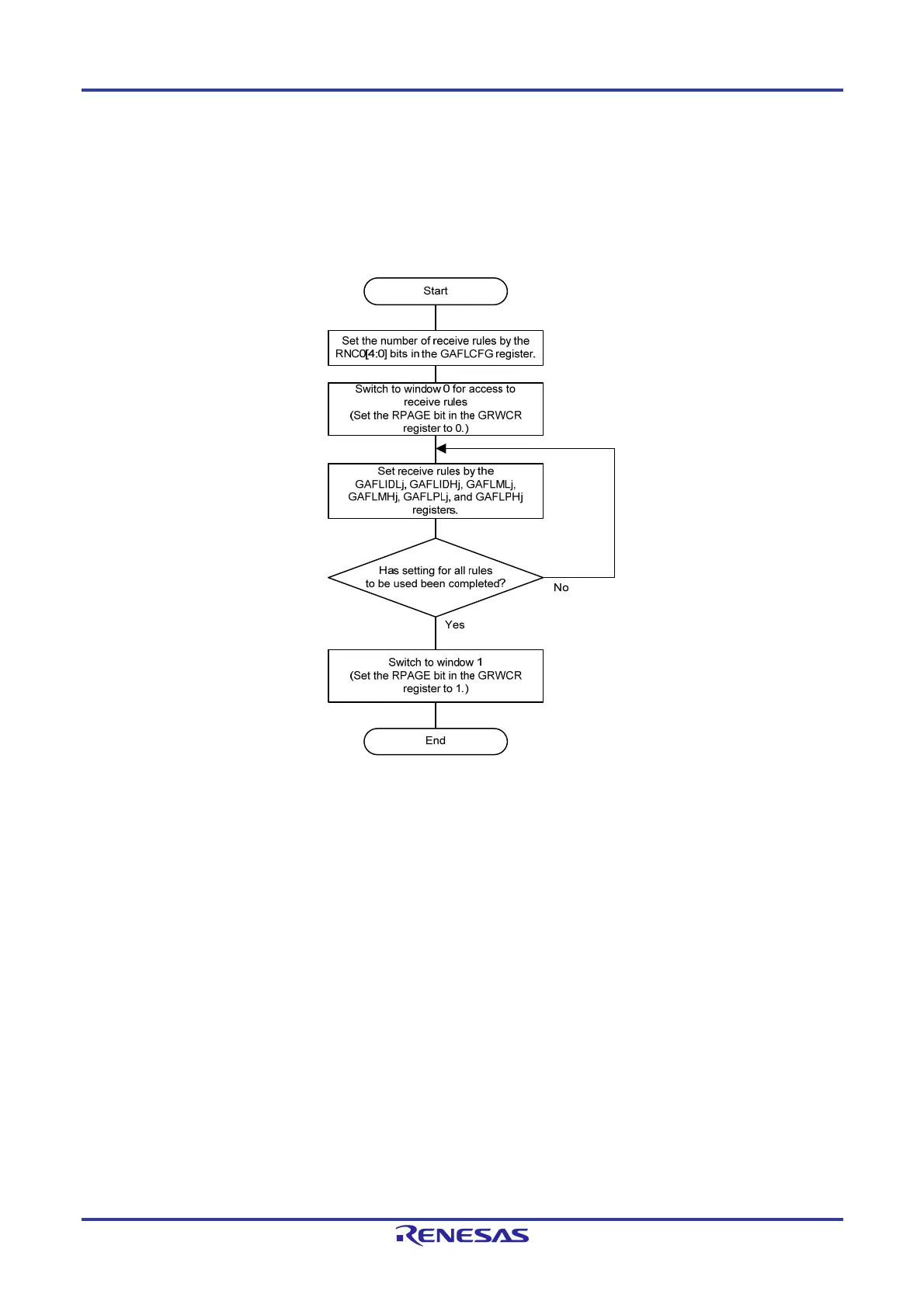
18.10.4 Receive Rule Setting
Receive rules can be set using receiv
e rule-related regist
ers.
Up to 16 receive rules can be register
ed.
Figure 18-19 shows the receive rule settin
g procedure.
Figure 18-19. Recei
ve Rule Setting Procedure
1438
1440
Table of Contents
Default Chapter
7
Table of Contents
7
Chapter 1 Overview
33
Features
33
Applications
34
Product Lineup
35
Function Overview
36
RL78/F14 Functions List
36
RL78/F13 (CAN and LIN Incorporated) Functions List
38
RL78/F13 (LIN Incorporated) Functions List
40
Block Diagram
42
RL78/F14: Block Diagram of R5F10Ppn (N = E, F, G, H, J) 100-Pin Products
42
RL78/F14: Block Diagram of R5F10Pmn (N = G, H, J) 80-Pin Products
43
RL78/F14: Block Diagram of R5F10Pln (N = G, H, J) 64-Pin Products
44
RL78/F14: Block Diagram of R5F10Pgn (N = G, H, J) 48-Pin Products
45
RL78/F14: Block Diagram of R5F10Pmn (N = E, F) 80-Pin Products
46
RL78/F14: Block Diagram of R5F10Pln (N = E, F) 64-Pin Products
47
RL78/F14: Block Diagram of R5F10Pgn (N = D, E, F) 48-Pin Products
48
RL78/F14: Block Diagram of R5F10Pbn (N = D, E) 32-Pin Products
49
RL78/F14: Block Diagram of R5F10Pan (N = D, E) 30-Pin Products
50
80-Pin Products
51
RL78/F13: Block Diagram of R5F10Bmn (N = E, F, G) (CAN and LIN Incorporated) 80-Pin Products
51
64-Pin Products
52
RL78/F13: Block Diagram of R5F10Bln (N = C, D, E, F, G) (CAN and LIN Incorporated) 64-Pin Products
52
RL78/F13: Block Diagram of R5F10Bgn (N = C, D, E, F, G) (CAN and LIN Incorporated) 48-Pin Products
53
RL78/F13: Block Diagram of R5F10Bbn (N = C, D, E, F, G) (CAN and LIN Incorporated) 32-Pin Products
54
RL78/F13: Block Diagram of R5F10Ban (N = C, D, E, F, G) (CAN and LIN Incorporated) 30-Pin Products
55
30-Pin Products
55
RL78/F13: Block Diagram of R5F10Amn (N = E, F, G) (LIN Incorporated) 80-Pin Products
56
RL78/F13: Block Diagram of R5F10Aln (N = F, G) (LIN Incorporated) 64-Pin Products
57
RL78/F13: Block Diagram of R5F10Agn (N = F, G) (LIN Incorporated) 48-Pin Products
58
RL78/F13: Block Diagram of R5F10Aln (N = C, D, E) (LIN Incorporated) 64-Pin Products
59
RL78/F13: Block Diagram of R5F10Agn (N = A, C, D, E) (LIN Incorporated) 48-Pin Products
60
RL78/F13: Block Diagram of R5F10Abn (N = A, C, D, E) (LIN Incorporated) 32-Pin Products
61
RL78/F13: Block Diagram of R5F10Aan (N = A, C, D, E) (LIN Incorporated) 30-Pin Products
62
RL78/F13: Block Diagram of R5F10A6N (N = A, C, D, E) (LIN Incorporated) 20-Pin Products
63
Pin Configurations
64
RL78/F14 Pin Configuration for 100-Pin Products
64
RL78/F14 Pin Configuration for 80-Pin Products
65
RL78/F13 Pin Configuration for 80-Pin Products
66
RL78/F14 Pin Configuration for 64-Pin Products
67
RL78/F13 Pin Configuration for 64-Pin Product
68
RL78/F14 Pin Configuration for 48-Pin Products
69
RL78/F13 Pin Configuration for 48-Pin Products
70
RL78/F14 Pin Configuration for 32-Pin Products
71
RL78/F13 Pin Configuration for 32-Pin Products
72
RL78/F14 Pin Configuration for 30-Pin Products
73
RL78/F13 Pin Configuration for 30-Pin Products
74
RL78/F13 Pin Configuration for 20-Pin Products
75
Order Information
76
Chapter 2 Pin Functions
79
Pin Function List
79
RL78/F14 100-Pin Products
81
RL78/F13 (CAN and LIN Incorporated) 80-Pin Products
83
RL78/F13 (LIN Incorporated) 80-Pin Products
85
Pins for each Product (Pins Other than Port Pins)
87
Description of Pin Functions
100
P00 to P03 (Port 0)
100
P10 to P17 (Port 1)
100
P30 to P34 (Port 3)
102
P40 to P47 (Port 4)
103
P50 to P57 (Port 5)
104
P60 to P67 (Port 6)
105
P70 to P77 (Port 7)
107
P80 to P87 (Port 8)
108
P90 to P97 (Port 9)
109
P100 to P107 (Port 10)
109
P120 to P127 (Port 12)
110
P130, P137 (Port 13)
111
P140 (Port 14)
111
P150 to P157 (Port 15)
112
VDD, Evdd0, Evdd1, Vss, Evss0, Evss1
112
Reset
113
Regc
113
Recommended Connection of Unused Pins
114
Chapter 3 Cpu Architecture
120
Memory Space
120
Internal Program Memory Space
146
Mirror Area
150
Internal Data Memory Space
152
Special Function Register (SFR) Area
153
Extended Special Function Register (2Nd SFR: 2Nd Special Function Register) Area
153
Data Memory Addressing
154
Processor Registers
172
Control Registers
172
General-Purpose Registers
175
ES and CS Registers
177
Special Function Registers (Sfrs)
178
Extended Special Function Registers (2Nd Sfrs: 2Nd Special Function Registers)
183
Instruction Address Addressing
216
Relative Addressing
216
Immediate Addressing
216
Table Indirect Addressing
217
Register Direct Addressing
218
Addressing for Processing Data Addresses
219
Implied Addressing
219
Register Addressing
219
Direct Addressing
220
Short Direct Addressing
221
SFR Addressing
222
Register Indirect Addressing
223
Based Addressing
224
Based Indexed Addressing
228
Stack Addressing
229
Chapter 4 Port Functions
233
Port Functions
233
Port Configuration
235
Port 0
236
Port 1
241
Port 3
252
Port 4
258
Port 5
268
Port 6
278
Port 7
288
Port 8
302
Port 9
312
Port 10
315
Port 12
320
Port 13
327
Port 14
330
Port 15
332
Registers Controlling Port Function
339
Port Mode Registers (Pmxx)
351
Port Registers (Pxx)
352
Pull-Up Resistor Option Registers (Puxx)
354
Port Input Mode Registers (PIM1, PIM3, PIM5 to PIM7, PIM12)
355
Port Output Mode Registers (POM1, POM6, POM7, POM12)
356
Port Mode Control Registers 7, 9, 12 (PMC7, PMC9, PMC12)
357
A/D Port Configuration Register (ADPC)
358
Port Input Threshold Control Register
360
(PITHL1, PITHL3 to PITHL7, PITHL10, PITHL12, PITHL15)
360
Peripheral I/O Redirection Register 0 (PIOR0)
362
Peripheral I/O Redirection Register 1 (PIOR1)
363
Peripheral I/O Redirection Register 2 (PIOR2)
364
Peripheral I/O Redirection Register 3 (PIOR3)
365
Peripheral I/O Redirection Register 4 (PIOR4)
366
Peripheral I/O Redirection Register 5 (PIOR5)
368
Peripheral I/O Redirection Register 6 (PIOR6)
369
Peripheral I/O Redirection Register 7 (PIOR7)
370
Peripheral I/O Redirection Register 8 (PIOR8)
371
Port Output Slew Rate Register (PSRSEL)
372
SNOOZE Status Output Control Register 0 (PSNZCNT0)
373
SNOOZE Status Output Control Register 1 (PSNZCNT1)
374
SNOOZE Status Output Control Register 2 (PSNZCNT2)
375
SNOOZE Status Output Control Register 3 (PSNZCNT3)
376
Port Mode Select Register (PMS)
377
Port Function Operations
378
Writing to I/O Port
378
Reading from I/O Port
378
Operations on I/O Port
378
Connecting to External Device with Different Potential (3 V)
379
Settings of Port Mode Register and Output Latch When Using Alternate Function
381
Cautions When Using Port Function
392
Cautions on 1-Bit Manipulation Instruction for Port Register N (Pn)
392
Notes on Specifying the Pin Settings
393
Chapter 5 Clock Generator
394
Functions of Clock Generator
394
Configuration of Clock Generator
397
Registers Controlling Clock Generator
401
Clock Operation Mode Control Register (CMC)
401
System Clock Control Register (CKC)
404
Clock Operation Status Control Register (CSC)
406
Oscillation Stabilization Time Counter Status Register (OSTC)
407
Oscillation Stabilization Time Select Register (OSTS)
409
Peripheral Enable Registers 0, 1, 2 (PER0, PER1, PER2)
411
Operation Speed Mode Control Register (OSMC)
417
High-Speed On-Chip Oscillator Frequency Select Register (HOCODIV)
418
High-Speed On-Chip Oscillator Trimming Register (HIOTRM)
419
CAN Clock Select Register (CANCKSEL)
420
LIN Clock Select Register (LINCKSEL)
421
Clock Select Register (CKSEL)
422
PLL Control Register (PLLCTL)
423
PLL Status Register (PLLSTS)
425
Fmp Clock Division Register (MDIV)
426
System Clock Oscillator
427
X1 Oscillator
427
XT1 Oscillator
427
High-Speed On-Chip Oscillator
431
PLL Circuit
431
Low-Speed On-Chip Oscillator
431
WDT-Dedicated Low-Speed On-Chip Oscillator
431
Clock Generator Operation
432
Controlling Clock
434
Example of Setting High-Speed On-Chip Oscillator
434
Example of Setting X1 Oscillator
436
Example of Setting XT1 Oscillator
437
Examples of Setting PLL Circuit
438
Example of Setting Low-Speed On-Chip Oscillator
440
CPU Clock Status Transition Diagram
441
Conditions before Changing CPU Clock and Processing after Changing CPU Clock
445
Main System Clock
452
Conditions before Clock Oscillation Is Stopped
454
Usage Notes
455
Cpu/Peripheral Hardware Clock
455
High-Speed On-Chip Oscillator
455
Chapter 6 Timer Array Unit
456
Functions of Timer Array Unit
458
Simultaneous Channel Operation Function
459
Bit Timer Operation Function (Channels 1 and 3 Only)
460
LIN-Bus Supporting Function (Channel 7 of Unit 0 Only)
461
Configuration of Timer Array Unit
462
Timer Count Register Mn (Tcrmn)
468
Timer Data Register Mn (Tdrmn)
470
Registers Controlling Timer Array Unit
471
Peripheral Enable Register 0 (PER0)
472
Timer Clock Select Register M (Tpsm)
473
Timer Mode Register Mn (Tmrmn)
476
Timer Status Register Mn (Tsrmn)
482
Timer Channel Enable Status Register M (Tem)
483
Timer Channel Start Register M (Tsm)
484
Timer Channel Stop Register M (Ttm)
485
Timer Input Select Register 0 (TIS0)
486
Timer Input Select Register 1 (TIS1)
487
Timer Input Select Register 2 (TIS2)
488
Timer Output Enable Register M (Toem)
489
Timer Output Register M (Tom)
490
Timer Output Level Register M (Tolm)
491
Timer Output Mode Register M (Tomm)
492
Noise Filter Enable Registers 1, 2 (NFEN1, NFEN2)
493
Port Mode Registers 1, 3, 4, 7, 12 (PM1, PM3, PM4, PM7, PM12)
496
PWM Output Delay Control Register 1 (PWMDLY1)
498
PWM Output Delay Control Register 2 (PWMDLY2)
499
Basic Rules of Timer Array Unit
500
Basic Rules of 8-Bit Timer Operation Function (Channels 1 and 3 Only)
502
Operation Timing of Counter
503
Start Timing of Counter
505
Operation of Counter
506
Channel Output (Tomn Pin) Control
511
Tomn Pin Output Setting
512
Cautions on Channel Output Operation
513
Collective Manipulation of Tomn Bit
518
Timer Interrupt and Tomn Pin Output at Operation Start
519
Independent Channel Operation Function of Timer Array Unit
520
Operation as External Event Counter
526
Operation as Frequency Divider
531
Operation as Input Pulse Interval Measurement
535
Operation as Input Signal High-/Low-Level Width Measurement
540
Operation as Delay Counter
545
Simultaneous Channel Operation Function of Timer Array Unit
550
Operation as PWM Function
558
Operation as Multiple PWM Output Function
565
Cautions When Using Timer Array Unit
574
Chapter 7 Timer Rj
575
I/O Pins
576
Registers
577
Peripheral Enable Register 1 (PER1)
578
Operation Speed Mode Control Register (OSMC)
579
Timer RJ Counter Register 0 (TRJ0), Timer RJ Reload Register
580
Timer RJ Control Register 0 (TRJCR0)
581
Timer RJ I/O Control Register 0 (TRJIOC0)
583
Timer RJ Mode Register 0 (TRJMR0)
585
Timer RJ Event Pin Select Register 0 (TRJISR0)
586
Port Mode Registers 1, 4 (PM1, PM4)
587
Operation
588
Timer Mode
589
Pulse Output Mode
590
Event Counter Mode
591
Pulse Width Measurement Mode
593
Pulse Period Measurement Mode
594
Coordination with Event Link Controller (ELC)
595
Notes on Timer RJ
596
Procedure for Setting Pins TRJO0 and TRJIO0
597
Functional Restriction in STOP Mode (Event Counter Mode Only)
598
Chapter 8 Timer Rd
599
Registers
601
Peripheral Enable Register 1 (PER1)
602
Clock Select Register (CKSEL)
603
Timer RD ELC Register (TRDELC)
604
Timer RD Start Register (TRDSTR)
605
Timer RD Mode Register (TRDMR)
606
Timer RD PWM Function Select Register (TRDPMR)
607
Timer RD Function Control Register (TRDFCR)
608
Timer RD Output Master Enable Register 1 (TRDOER1)
610
Timer RD Output Master Enable Register 2 (TRDOER2)
611
Timer RD Output Control Register (TRDOCR)
612
Timer RD Digital Filter Function Select Register I (Trddfi) (I = 0 or 1)
615
Timer RD Control Register I (Trdcri) (I = 0 or 1)
617
Timer RD I/O Control Register Ai (Trdiorai) (I = 0 or 1)
622
Timer RD I/O Control Register CI (Trdiorci) (I = 0 or 1)
624
Timer RD Status Register I (Trdsri) (I = 0 or 1)
626
Timer RD Interrupt Enable Register I (Trdieri) (I = 0 or 1)
630
Timer RD PWM Function Output Level Control Register I (Trdpocri) (I = 0 or 1)
631
Timer RD Counter I (Trdi) (I = 0 or 1)
632
Timer RD General Registers Ai, Bi, CI, and DI (Trdgrai, Trdgrbi,Trdgrci, Trdgrdi I = 0 or 1)
634
PWM Output Delay Control Register 0 (PWMDLY0)
643
Port Mode Registers (PM1, PM3, PM12)
644
Operation
645
Input Capture Function
656
Output Compare Function
660
PWM Function
665
Reset Synchronous PWM Mode
669
Complementary PWM Mode
672
PWM3 Mode
676
Timer RD Interrupt
679
Notes on Timer RD
681
Count Source
682
Reset Synchronous PWM Mode
683
Chapter 9 Real-Time Clock
688
Registers Controlling Real-Time Clock
690
Peripheral Enable Register 0 (PER0)
691
Operation Speed Mode Control Register (OSMC)
692
Timer Input Select Register 1 (TIS1)
693
Timer Input Select Register 2 (TIS2)
694
RTC Clock Select Register (RTCCL)
695
Real-Time Clock Control Register 0 (RTCC0)
696
Real-Time Clock Control Register 1 (RTCC1)
697
Second Count Register (SEC)
699
Hour Count Register (HOUR)
700
Day Count Register (DAY)
702
Week Count Register (WEEK)
703
Month Count Register (MONTH)
704
Watch Error Correction Register (SUBCUD)
705
Bit Watch Error Correction Register (SUBCUDW)
706
Alarm Minute Register (ALARMWM)
707
Real-Time Clock Operation
709
Shifting to HALT/STOP Mode after Starting Operation
710
Reading/Writing Real-Time Clock
711
Setting Alarm of Real-Time Clock
713
Hz Output of Real-Time Clock
714
Example of Watch Error Correction of Real-Time Clock
715
Chapter 10 Clock Output/Buzzer Output Controller
718
Configuration of Clock Output/Buzzer Output Controller
720
Clock Select Register (CKSEL)
722
Port Mode Register 14 (PM14)
723
Operations of Clock Output/Buzzer Output Controller
724
Chapter 11 Watchdog Timer
725
Configuration of Watchdog Timer
726
Register Controlling Watchdog Timer
727
Operation of Watchdog Timer
728
Setting Overflow Time of Watchdog Timer
729
Setting Window Open Period of Watchdog Timer
730
Setting Watchdog Timer Interval Interrupt
731
Chapter 12 A/D Converter
732
Function of A/D Converter
733
Configuration of A/D Converter
735
Registers Used in A/D Converter
737
Peripheral Enable Register 0 (PER0)
738
A/D Converter Mode Register 0 (ADM0)
739
A/D Converter Mode Register 1 (ADM1)
748
A/D Converter Mode Register 2 (ADM2)
749
Bit A/D Conversion Result Register (ADCR)
752
Bit A/D Conversion Result Register (ADCRH)
753
Analog Input Channel Specification Register (ADS)
754
Conversion Result Comparison Upper Limit Setting Register (ADUL)
757
A/D Test Register (ADTES)
758
A/D Port Configuration Register (ADPC)
759
A/D Converter Trigger Select Register 0 (ADTRGS0) (RL78/F13 Only)
760
A/D Converter Trigger Select Register 1 (ADTRGS1) (RL78/F13 Only)
761
Port Mode Control Registers 7, 9, and 12 (PMC7, PMC9, PMC12)
762
Port Mode Registers 3, 7 to 10, and 12 (PM3, PM7 to PM10, PM12)
763
A/D Converter Conversion Operations
765
Input Voltage and Conversion Results
767
A/D Converter Operation Modes
768
Software Trigger Mode (Select Mode, One-Shot Conversion Mode)
769
Software Trigger Mode (Scan Mode, Sequential Conversion Mode)
770
Software Trigger Mode (Scan Mode, One-Shot Conversion Mode)
771
Hardware Trigger No-Wait Mode (Select Mode, Sequential Conversion Mode)
772
Hardware Trigger No-Wait Mode (Select Mode, One-Shot Conversion Mode)
773
Hardware Trigger No-Wait Mode (Scan Mode, Sequential Conversion Mode)
774
Hardware Trigger No-Wait Mode (Scan Mode, One-Shot Conversion Mode)
775
Hardware Trigger Wait Mode (Select Mode, Sequential Conversion Mode)
776
Hardware Trigger Wait Mode (Select Mode, One-Shot Conversion Mode)
777
Hardware Trigger Wait Mode (Scan Mode, Sequential Conversion Mode)
778
Hardware Trigger Wait Mode (Scan Mode, One-Shot Conversion Mode)
779
A/D Converter Setup Flowchart
780
Setting up Software Trigger Mode
781
Setting up Hardware Trigger No-Wait Mode
782
Setting up Hardware Trigger Wait Mode
783
Setting up Test Mode
785
SNOOZE Mode Function
786
If an Interrupt Is Generated after A/D Conversion Ends
787
If no Interrupt Is Generated after A/D Conversion Ends
788
How to Read A/D Converter Characteristics Table
789
Cautions for A/D Converter
791
CHAPTER 13 D/A CONVERTER (RL78/F14 Only)
795
Configuration of D/A Converter
796
Registers of D/A Converter
797
A/D Port Configuration Register (ADPC)
798
Peripheral Enable Register 1 (PER1)
799
D/A Converter Mode Register (DAM)
800
D/A Converter Mode Register 2 (DAM2)
801
D/A Conversion Value Setting Register 0 (DACS0)
802
Port Mode Register 8 (PM8)
803
Operations of D/A Converter
805
Operation in Real-Time Output Mode
806
Cautions for D/A Converter
807
CHAPTER 14 COMPARATOR (RL78/F14 Only)
808
Registers to Control the Comparator
810
Comparator Control Register (CMPCTL)
811
Comparator I/O Select Register (CMPSEL)
813
Comparator Output Monitor Register (CMPMON)
814
A/D Port Configuration Register (ADPC)
815
D/A Converter Mode Register 2 (DAM2)
816
Port Mode Register 4 (PM4)
817
Port Mode Register (PM8)
818
Operation
819
Noise Filter
820
Comparator Interrupts
821
Comparator Setting Flowchart
822
Chapter 15 Serial Array Unit
824
Functions of Serial Array Unit
825
Uart (Uart0, Uart1)
826
Configuration of Serial Array Unit
828
Registers Controlling Serial Array Unit
834
Peripheral Enable Register 0 (PER0)
835
Serial Clock Select Register M (Spsm)
836
Serial Mode Register Mn (Smrmn)
837
Serial Communication Operation Setting Register Mn (Scrmn)
839
Higher 7 Bits of the Serial Data Register Mn (Sdrmn)
842
Serial Flag Clear Trigger Register Mn (Sirmn)
844
Serial Status Register Mn (Ssrmn)
845
Serial Channel Start Register M (Ssm)
847
Serial Channel Stop Register M (Stm)
848
Serial Channel Enable Status Register M (Sem)
849
Serial Output Enable Register M (Soem)
850
Serial Output Register M (Som)
851
Serial Output Level Register M (Solm)
852
Serial Slave Select Enable Register M (Ssem)
853
Input Switch Control Register (ISC)
854
Noise Filter Enable Register 0 (NFEN0)
855
Port Input Mode Registers 1, 3, 5 to 7, 12 (PIM1, PIM3, PIM5 to PIM7, PIM12)
856
Port Output Mode Registers 1, 6, 7, 12 (POM1, POM6, POM7, POM12)
857
Port Mode Registers 1, 3 to 7, 12 (PM1, PM3 to PM7, PM12)
858
Operation Stop Mode
860
Stopping the Operation by Units
861
Stopping the Operation by Channels
862
Operation of 3-Wire Serial I/O (CSI00, CSI01, CSI10, CSI11) Communication
864
Master Transmission
866
Master Reception
876
Master Transmission/Reception
886
Slave Transmission
896
Slave Reception
906
Slave Transmission/Reception
913
Calculating Transfer Clock Frequency
923
Procedure for Processing Errors that Occurred During 3-Wire Serial I/O CSI00, CSI01, CSI10, CSI11) Communication
925
Clock Synchronous Serial Communication with SPI Function
926
Master Transmission
930
Master Reception
940
Master Transmission/Reception
950
Slave Transmission
960
Slave Reception
970
Slave Transmission/Reception
977
Calculating Transfer Clock Frequency
987
Procedure for Processing Errors that Occurred During Clock Synchronous Serial Communication with SPI Function
989
Operation of UART (UART0, UART1) Communication
990
UART Transmission
992
UART Reception
1002
Calculating Baud Rate
1009
Procedure for Processing Errors that Occurred During UART (UART0, UART1) Communication
1013
LIN Communication Operation
1014
LIN Reception
1017
Address Field Transmission
1026
Data Transmission
1032
Data Reception
1037
Stop Condition Generation
1042
Calculating Transfer Rate
1044
Chapter 16 Serial Interface Iica
1048
Configuration of Serial Interface IICA
1051
Registers Controlling Serial Interface IICA
1054
IICA Control Register 00 (IICCTL00)
1055
IICA Status Register 0 (IICS0)
1060
IICA Flag Register 0 (IICF0)
1062
IICA Control Register 01 (IICCTL01)
1064
IICA Low-Level Width Setting Register 0 (IICWL0)
1066
Port Mode Register 6 (PM6)
1067
Port Output Mode Register (POM6)
1068
Pin Configuration
1069
Setting Transfer Clock by Using IICWL0 and IICWH0 Registers
1070
Start Conditions
1072
Addresses
1073
Acknowledge (ACK)
1074
Stop Condition
1075
Wait
1076
Canceling Wait
1078
Interrupt Request (INTIICA0) Generation Timing and Wait Control
1079
Address Match Detection Method
1080
Arbitration
1081
Wakeup Function
1083
Communication Reservation
1086
Cautions
1090
Communication Operations
1091
Timing Charts
1119
Chapter 17 Lin/Uart Module (Rlin3)
1134
Register Descriptions
1139
LIN Registers for Master Mode
1141
LIN Registers for Slave Mode
1169
Registers for UART
1197
Modes
1227
LIN Reset Mode
1229
LIN Mode
1230
UART Mode
1232
LIN Mode
1233
Data Transmission/Reception
1241
Transmission/Reception Data Buffering
1243
Wake-Up Transmission/Reception
1246
Status
1248
Error Status
1250
UART Mode
1256
Data Transmission/Reception
1271
Buffer Processing of Transmission Data
1273
Status
1274
Error Status
1275
LIN Self-Test Mode
1276
Change to LIN Self-Test Mode
1277
Transmission in LIN Master Self-Test Mode
1278
Reception in LIN Master Self-Test Mode
1279
Transmission in LIN Slave Self-Test Mode
1280
Reception in LIN Slave Self-Test Mode
1281
Terminating LIN Self-Test Mode
1282
Baud Rate Generator
1283
LIN Slave Mode
1285
UART Mode
1287
Noise Filter
1288
Interrupts
1290
Chapter 18 Can Interface (Rs-Can Lite)
1291
Input/Output Pins
1294
Register Descriptions
1295
Cani Bit Configuration Register L (Cicfgl) (I = 0)
1317
Cani Bit Configuration Register H (Cicfgh) (I = 0)
1318
Cani Control Register L (Cictrl) (I = 0)
1320
Cani Control Register H (Cictrh) (I = 0)
1322
Cani Status Register L (Cistsl) (I = 0)
1324
Cani Status Register H (Cistsh) (I = 0)
1326
Cani Error Flag Register L (Cierfll) (I = 0)
1327
Cani Error Flag Register H (Cierflh) (I = 0)
1330
CAN Global Configuration Register L (GCFGL)
1331
CAN Global Configuration Register H (GCFGH)
1333
CAN Global Control Register L (GCTRL)
1334
CAN Global Control Register H (GCTRH)
1335
CAN Global Status Register (GSTS)
1336
CAN Global Error Flag Register (GERFLL)
1337
CAN Global Transmit Interrupt Status Register (GTINTSTS)
1338
CAN Timestamp Register (GTSC)
1339
CAN Receive Rule Number Configuration Register (GAFLCFG)
1340
CAN Receive Rule Entry Register Jal (Gaflidlj) (J = 0 to 15)
1341
CAN Receive Rule Entry Register Jah (Gaflidhj) (J = 0 to 15)
1342
CAN Receive Rule Entry Register Jbl (Gaflmlj) (J = 0 to 15)
1343
CAN Receive Rule Entry Register Jbh (Gaflmhj) (J = 0 to 15)
1344
CAN Receive Rule Entry Register Jcl (Gaflplj) (J = 0 to 15)
1345
CAN Receive Rule Entry Register Jch (Gaflphj) (J = 0 to 15)
1346
CAN Receive Buffer Number Configuration Register (RMNB)
1347
CAN Receive Buffer Receive Complete Flag Register (RMND0)
1348
CAN Receive Buffer Register Nal (Rmidln) (N = 0 to 15)
1349
CAN Receive Buffer Register Nah (Rmidhn) (N = 0 to 15)
1350
CAN Receive Buffer Register Nbl (Rmtsn) (N = 0 to 15)
1351
CAN Receive Buffer Register Nbh (Rmptrn) (N = 0 to 15)
1352
CAN Receive Buffer Register Ncl (Rmdf0N) (N = 0 to 15)
1353
CAN Receive Buffer Register Nch (Rmdf1N) (N = 0 to 15)
1354
CAN Receive Buffer Register Ndl (Rmdf2N) (N = 0 to 15)
1355
CAN Receive Buffer Register Ndh (Rmdf3N) (N = 0 to 15)
1356
CAN Receive FIFO Control Register M (Rfccm) (M = 0, 1)
1357
CAN Receive FIFO Status Register M (Rfstsm) (M = 0, 1)
1359
CAN Receive FIFO Pointer Control Register M (Rfpctrm) (M = 0, 1)
1361
CAN Receive FIFO Access Register Mal (Rfidlm) (M = 0, 1)
1362
CAN Receive FIFO Access Register Mah (Rfidhm) (M = 0, 1)
1363
CAN Receive FIFO Access Register Mbl (Rftsm) (M = 0, 1)
1364
CAN Receive FIFO Access Register Mbh (Rfptrm) (M = 0, 1)
1365
CAN Receive FIFO Access Register Mcl (Rfdf0M) (M = 0, 1)
1366
CAN Receive FIFO Access Register Mch (Rfdf1M) (M = 0, 1)
1367
CAN Receive FIFO Access Register Mdl (Rfdf2M) (M = 0, 1)
1368
CAN Receive FIFO Access Register Mdh (Rfdf3M) (M = 0, 1)
1369
Cani Transmit/Receive FIFO Control Register Kl (Cfcclk) (I = 0) (K = 0)
1370
Cani Transmit/Receive FIFO Control Register Kh (Cfcchk) (I = 0) (K = 0)
1372
Cani Transmit/Receive FIFO Status Register K (Cfstsk) (I = 0) (K = 0)
1374
Cani Transmit/Receive FIFO Pointer Control Register K (Cfpctrk) (I = 0) (K = 0)
1376
Cani Transmit/Receive FIFO Access Register Kal (Cfidlk) (I = 0) (K = 0)
1377
Cani Transmit/Receive FIFO Access Register Kah (Cfidhk) (I = 0) (K = 0)
1378
Cani Transmit/Receive FIFO Access Register Kbl (Cftsk) (I = 0) (K = 0)
1379
Cani Transmit/Receive FIFO Access Register Kbh (Cfptrk) (I = 0) (K = 0)
1380
Cani Transmit/Receive FIFO Access Register Kcl (Cfdf0K) (I = 0) (K = 0)
1381
Cani Transmit/Receive FIFO Access Register Kch (Cfdf1K) (I = 0) (K = 0)
1382
Cani Transmit/Receive FIFO Access Register Kdl (Cfdf2K) (I = 0) (K = 0)
1383
Cani Transmit/Receive FIFO Access Register Kdh (Cfdf3K) (I = 0) (K = 0)
1384
Receive FIFO Message Lost Status Register (RFMSTS)
1385
Cani Transmit/Receive FIFO Message Lost Status Register (CFMSTS) (I = 0)
1386
CAN Receive FIFO Interrupt Status Register (RFISTS)
1387
CAN Transmit/Receive FIFO Receive Interrupt Status Register (CFISTS)
1388
Cani Transmit Buffer Control Register P (Tmcp) (I = 0) (P = 0 to 3)
1389
Cani Transmit Buffer Status Register P (Tmstsp) (I = 0) (P = 0 to 3)
1391
Cani Transmit Buffer Transmit Request Status Register (TMTRSTS) (I = 0)
1392
Cani Transmit Buffer Transmit Complete Status Register (TMTCSTS) (I = 0)
1393
Cani Transmit Buffer Transmit Abort Status Register (TMTASTS) (I = 0)
1394
Cani Transmit Buffer Interrupt Enable Register (TMIEC) (I = 0)
1395
Cani Transmit Buffer Register Pal (Tmidlp) (I = 0) (P = 0 to 3)
1396
Cani Transmit Buffer Register Pah (Tmidhp) (I = 0) (P = 0 to 3)
1397
Cani Transmit Buffer Register Pbh (Tmptrp) (I = 0) (P = 0 to 3)
1398
Cani Transmit Buffer Register Pcl (Tmdf0P) (I = 0) (P = 0 to 3)
1399
Cani Transmit Buffer Register Pch (Tmdf1P) (I = 0) (P = 0 to 3)
1400
Cani Transmit Buffer Register Pdl (Tmdf2P) (I = 0) (P = 0 to 3)
1401
Cani Transmit Buffer Register Pdh (Tmdf3P) (I = 0) (P = 0 to 3)
1402
Cani Transmit History Buffer Control Register (Thlcci) (I = 0)
1403
Cani Transmit History Buffer Status Register (Thlstsi) (I = 0)
1404
Cani Transmit History Buffer Access Register (Thlacci) (I = 0)
1405
Cani Transmit History Buffer Pointer Control Register (Thlpctri) (I = 0)
1406
CAN Global RAM Window Control Register (GRWCR)
1407
CAN Global Test Configuration Register (GTSTCFG)
1408
CAN Global Test Control Register (GTSTCTRL)
1409
CAN Global Test Protection Unlock Register (GLOCKK)
1410
CAN RAM Test Register R (Rpgaccr) (R = 0 to 127)
1411
CAN Modes
1412
Channel Modes
1414
Reception Function
1419
Timestamp
1421
Transmission Functions
1422
Transmission Using Transmit Buffers
1423
Transmission Using FIFO Buffers
1424
Transmit History Function
1426
Test Function
1427
Self-Test Mode (Loopback Mode)
1428
Interrupt
1429
RAM Window
1433
Initial Settings
1434
Clock Setting
1436
Communication Speed Setting
1437
Receive Rule Setting
1439
Buffer Setting
1440
Reception Procedure
1442
FIFO Buffer Reading Procedure
1444
Transmission Procedure
1447
Procedure for Transmission from Transmit/Receive FIFO Buffers
1450
Transmit History Buffer Reading Procedure
1453
Test Settings
1454
Protection Unlock Procedure
1455
RAM Test Setting Procedure
1456
Notes on the CAN Module
1457
Chapter 19 Dtc
1458
Registers
1460
Allocation of DTC Control Data Area and DTC Vector Table Area
1462
DTC Control Data Allocation
1463
DTC Vector Table
1464
Peripheral Enable Register 1 (PER1)
1468
DTC Activation Enable Register I (Dtceni) (I = 0 to 5)
1469
DTC Base Address Register (DTCBAR)
1472
DTC Control Register J (Dtccrj) (J = 0 to 23)
1473
DTC Block Size Register J (Dtblsj) (J = 0 to 23)
1474
DTC Transfer Count Reload Register J (Dtrldj) (J = 0 to 23)
1475
High-Speed DTC Channel Select Register 0 (SELHS0)
1476
High-Speed DTC Channel Select Register 1 (SELHS1)
1477
High-Speed DTC Control Register M (HDTCCR0/1) (M = 0, 1)
1478
High-Speed DTC Transfer Count Register M (HDTCCT0/1) (M = 0, 1)
1479
DTC Transfer Count Reload Register M (HDTRLD0/1) (M = 0, 1)
1480
Operation
1481
Normal Mode
1483
Repeat Mode
1485
Chain Transfers
1489
High-Speed Transfer Operation
1491
Notes on DTC
1492
DTC Pending Instruction
1493
Number of DTC Execution Clock Cycles
1494
Number of High-Speed DTC Execution Clock Cycles
1495
DTC Response Time
1496
Operation in Standby Mode Status
1497
CHAPTER 20 EVENT LINK CONTROLLER (ELC) (RL78/F14 Only)
1498
Registers
1499
Event Output Destination Select Register N (Elselrn) (N = 00 to 25)
1500
Timer Input Select Register 0
1503
Operation
1504
Chapter 21 Interrupt Functions
1505
Interrupt Sources and Configuration
1506
Registers Controlling Interrupt Functions
1516
Interrupt Request Flag Registers (IF0L, IF0H, IF1L, IF1H, IF2L, IF2H, IF3L)
1522
Interrupt Mask Flag Registers (MK0L, MK0H, MK1L, MK1H, MK2L, MK2H, MK3L)
1524
Priority Specification Flag Registers (PR00L, PR00H, PR01L, PR01H, PR02L, PR02H, PR03L PR10L, PR10H, PR11L, PR11H, PR12L, PR12H, PR13L)
1526
External Interrupt Rising Edge Enable Registers (EGP0, EGP1 External Interrupt Falling Edge Enable Registers (EGN0, EGN1)
1529
Interrupt Source Determination Flag Register 0 (INTFLG0)
1531
Interrupt Mask Register (INTMSK)
1534
Input Switch Control Register (ISC)
1535
Program Status Word (PSW)
1536
Interrupt Servicing Operations
1537
Software Interrupt Request Acknowledgment
1540
Interrupt Servicing During Division Instruction
1544
Interrupt Request Hold
1546
Chapter 22 Key Interrupt Function
1547
Configuration of Key Interrupt
1548
Register Controlling Key Interrupt
1549
Chapter 23 Standby Function
1550
Registers Controlling Standby Function
1551
Oscillation Stabilization Time Counter Status Register (OSTC)
1552
Oscillation Stabilization Time Select Register (OSTS)
1553
STOP Status Output Control Register (STPSTC)
1554
Standby Function Operation
1555
STOP Mode
1562
SNOOZE Mode
1568
Chapter 24 Reset Function
1573
Register for Confirming Reset Source
1584
POR/CLM Reset Confirmation Register (POCRES)
1585
Chapter 25 Power-On-Reset Circuit
1587
Configuration of Power-On-Reset Circuit
1588
Cautions for Power-On-Reset Circuit
1591
Chapter 26 Voltage Detector
1593
Configuration of Voltage Detector
1594
Voltage Detection Register (LVIM)
1595
Voltage Detection Level Register (LVIS)
1596
Operation of Voltage Detector
1599
When Used as Interrupt Mode
1601
When Used as Interrupt and Reset Mode
1603
Cautions for Voltage Detector
1609
Delay from the Time LVD Reset Source Is Generated until the Time LVD Reset Has Been Generated or Released
1610
Chapter 27 Safety Functions
1611
Registers Used by Safety Functions
1613
Operation of Safety Functions
1614
CRC Operation Function (General-Purpose CRC)
1618
RAM-ECC Function
1622
CPU Stack Pointer Monitor Function
1628
Clock Monitor
1631
RAM Guard Function
1632
SFR Guard Function
1633
Invalid Memory Access Detection Function
1634
Frequency Detection Function
1637
A/D Test Function
1640
Digital Output Signal Level Detection Function for I/O Ports
1645
Chapter 28 Regulator
1646
Chapter 29 Option Byte
1647
On-Chip Debug Option Byte (000C3H/ 020C3H)
1648
Format of User Option Byte
1649
Format of On-Chip Debug Option Byte
1653
Setting of Option Byte
1654
Chapter 30 Flash Memory
1655
Serial Programming Using Flash Memory Programmer
1657
Programming Environment
1659
Serial Programming Using External Device (that Incorporates UART)
1661
Communication Mode
1662
Connection of Pins on Board
1663
Port Pins
1664
Serial Programming Method
1665
Flash Memory Programming Mode
1666
Selecting Communication Mode
1667
Communication Commands
1668
Processing Time for each Command When PG-FP5 Is in Use (Reference Value)
1669
Self-Programming
1670
Self-Programming Procedure
1671
Boot Swap Function
1672
Flash Shield Window Function
1674
Security Settings
1675
Data Flash
1677
Register Controlling Data Flash Memory
1678
Procedure for Accessing Data Flash Memory
1679
Chapter 31 On-Chip Debug Function
1680
Connecting E1 On-Chip Debugging Emulator to RL78/F13 or RL78/F14
1682
On-Chip Debug Security ID
1683
Chapter 32 Bcd Correction Circuit
1686
BCD Correction Circuit Operation
1687
Chapter 33 Instruction Set
1689
Conventions Used in Operation List
1690
Description of Operation Column
1691
Description of Flag Operation Column
1692
Operation List
1693
Chapter 34 Electrical Specifications (Grade L)
1711
Absolute Maximum Ratings
1712
Oscillator Characteristics
1714
On-Chip Oscillator Characteristics
1715
Subsystem Clock Oscillator Characteristics
1716
PLL Circuit Characteristics
1717
DC Characteristics
1718
Supply Current Characteristics
1724
AC Characteristics
1729
Peripheral Functions Characteristics
1732
Serial Interface IICA
1751
On-Chip Debug (UART)
1752
Analog Characteristics
1753
Temperatures Sensor Characteristics
1757
POR Circuit Characteristics
1758
LVD Circuit Characteristics
1759
Power Supply Voltage Rising Time
1760
Flash Memory Programming Characteristics
1761
Chapter 35 Electrical Specifications (Grade K)
1762
Absolute Maximum Ratings
1763
Oscillator Characteristics
1765
On-Chip Oscillator Characteristics
1766
Subsystem Clock Oscillator Characteristics
1767
PLL Circuit Characteristics
1768
DC Characteristics
1769
Supply Current Characteristics
1775
AC Characteristics
1780
Peripheral Functions Characteristics
1783
Serial Interface IICA
1802
On-Chip Debug (UART)
1803
Analog Characteristics
1804
Temperatures Sensor Characteristics
1808
POR Circuit Characteristics
1809
LVD Circuit Characteristics
1810
Power Supply Voltage Rising Time
1811
Flash Memory Programming Characteristics
1812
Chapter 36 Electrical Specifications (Grade Y)
1813
Absolute Maximum Ratings
1814
Oscillator Characteristics
1816
On-Chip Oscillator Characteristics
1817
Subsystem Clock Oscillator Characteristics
1818
PLL Circuit Characteristics
1819
DC Characteristics
1820
Supply Current Characteristics
1826
AC Characteristics
1831
Peripheral Functions Characteristics
1834
Serial Interface IICA
1853
On-Chip Debug (UART)
1854
Analog Characteristics
1855
Temperatures Sensor Characteristics
1859
POR Circuit Characteristics
1860
LVD Circuit Characteristics
1861
Power Supply Voltage Rising Time
1862
Flash Memory Programming Characteristics
1863
Appendix A Related Products
1872
Other manuals for Renesas RL78 Series
Application Note
53 pages
4
Based on 1 rating
Ask a question
Give review
Questions and Answers:
Need help?
Do you have a question about the Renesas RL78 Series and is the answer not in the manual?
Ask a question
Renesas RL78 Series Specifications
General
Brand
Renesas
Model
RL78 Series
Category
Computer Hardware
Language
English
Related product manuals
Renesas RL78/G13
1092 pages
Renesas RL78/F13
1879 pages
Renesas RL78/F14
1879 pages
Renesas RL78/D1A
1879 pages
Renesas RL78/G1D
1092 pages
Renesas RH850
67 pages
Renesas RX66T
25 pages
Renesas RZ/T2M
87 pages
Renesas EK-RA6M3
22 pages
Renesas RZ Series
83 pages
Renesas RZ/A Series
106 pages
Renesas RH850/F1KM-S4
26 pages
 Loading...


